In the ever-evolving world of semiconductor technology, innovation is the key to staying ahead. At Kurt J. Lesker Company, we are proud to announce a groundbreaking achievement that promises to revolutionize the field of Atomic Layer Deposition (ALD). Our latest publication, featuring the patented Precursor Focusing Technique (PFT) and Ultra-High Purity (UHP) process capability, marks a significant milestone in our commitment to advancing next-generation applications.

The First of Its Kind: Scandium Nitride by PEALD
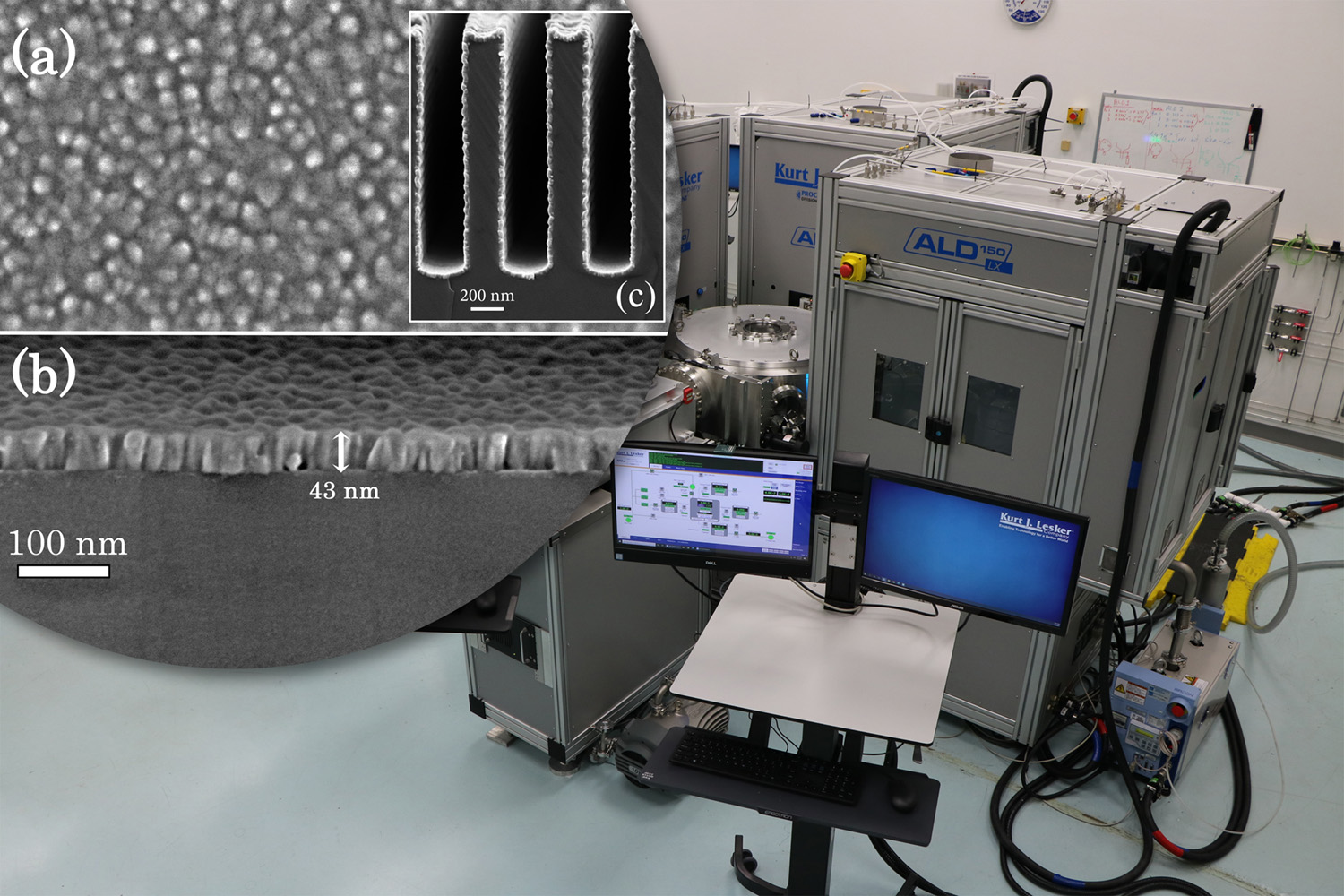
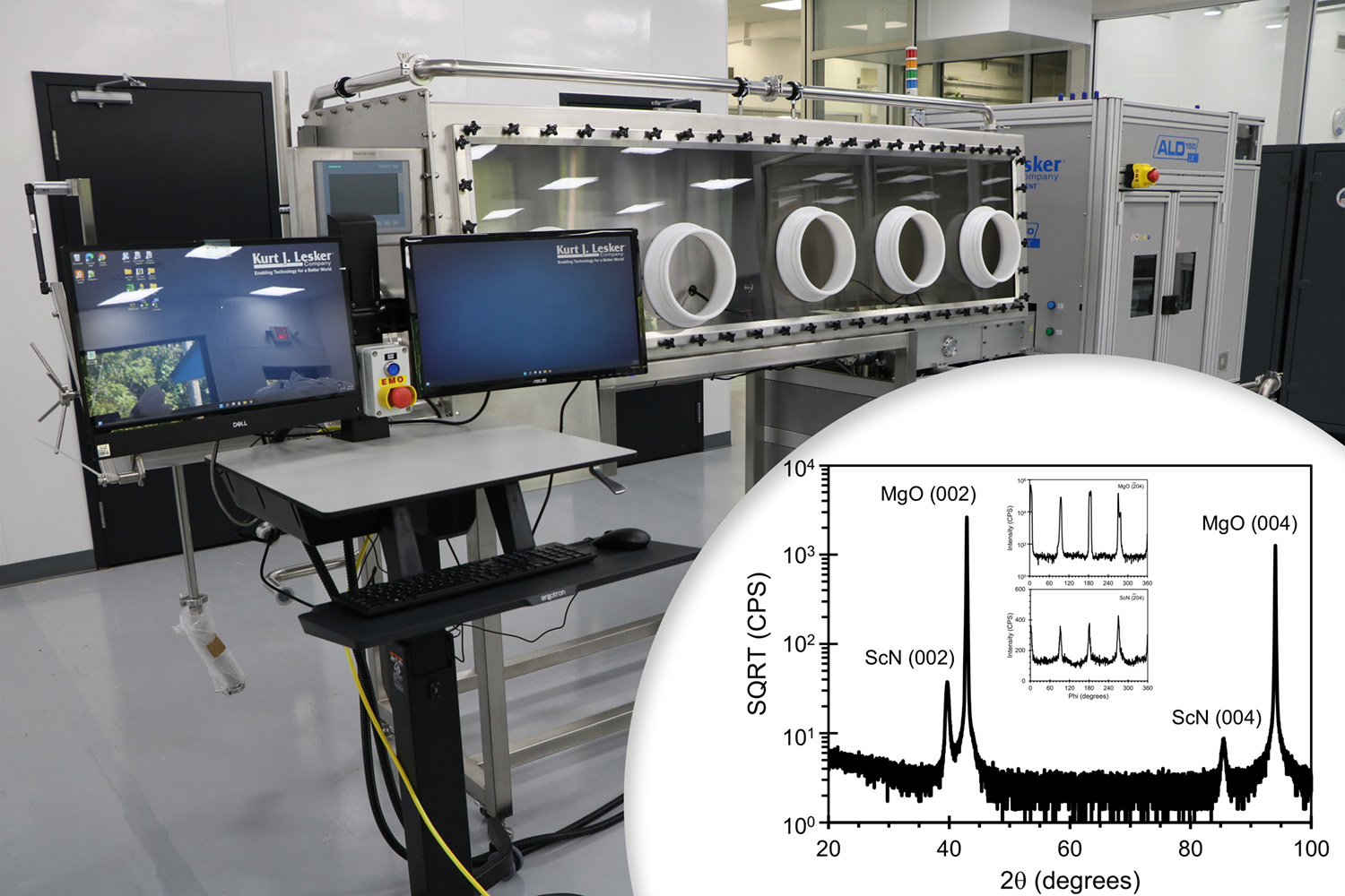
For the first time, scandium nitride (ScN) has been successfully deposited using plasma-enhanced atomic layer deposition (PEALD) on silicon, sapphire, and magnesium oxide substrates under UHP conditions. This innovative process utilizes a new scandium precursor, bis(ethylcyclopentadienyl)scandium-chloride [ClSc(EtCp)2], combined with N2-H2 plasma species, allowing for the deposition of high-quality ScN films at relatively low temperatures (200−300°C).

Why This Publication is a Game-Changer
The significance of this publication lies in its potential to transform various advanced electronic applications. The ScN films produced by this process exhibit high crystalline quality and excellent electrical properties, with high mobility and low resistivity. These characteristics make them suitable for a wide range of applications, including thermoelectric devices and as an interlayer for epitaxial gallium nitride (GaN) growth.
Moreover, the ability to conformally coat high aspect ratio (HAR) structures is particularly valuable for applications in 3D embedded memory and piezoelectric microelectromechanical systems (piezoMEMS). Traditional sputtering techniques are not suitable for these applications involving complex 3D architectures, making this new ALD process a significant advancement.

The Commercial Relevance of ScN
Scandium nitride is commercially relevant primarily because it forms a solid solution with aluminum nitride (AlN), resulting in aluminum scandium nitride (Al1-xScxN), which enables ferroelectric switching. Al1-xScxN thin films are traditionally deposited via reactive magnetron sputtering, which yields highly c-axis oriented columnar grains. However, sputtering is not suitable for coating high-aspect ratio (HAR), vertically layered structures such as those desired for use in 3D embedded memory.
Recently, there have been several reports of piezoelectric AlN grown by atomic layer deposition (ALD) techniques that have shown promising crystalline quality and properties. However, there are no reports of ALD Al1-xScxN, principally because there are no reported ALD processes for ScN. This publication addresses this gap, providing a new method for depositing high-quality ScN films.
Looking Ahead
As KJLC continues to push the boundaries of ALD technology, we are excited about the possibilities our new research and development opens up. From thermoelectrics to applications involving high-aspect ratio (HAR) architectures such as 3D embedded memory and piezoMEMS technology, the high crystalline and electrical quality demonstrated here for ScN by PEALD techniques is just the beginning.
For more information on the significance of scandium nitride and its applications, you can refer to the following resources:
- Read Ultrahigh purity plasma-enhanced atomic layer deposition and electrical properties of epitaxial scandium nitride on the Journal of Vacuum Science & Techology A
- How KJLC's ALD Systems are Powering Next Gen Research
- Download Manuscript
Stay tuned for more updates as we leverage this groundbreaking technology to drive sustainable business growth and maintain our leadership in the ALD market.
For more information, please use the "Contact Us Today" button below for the quickest way to get in contact with us.


