Dr. Kai Ni from the research group of Professor Suman Datta, Stinson Professor of Nanotechnology at the University of Notre Dame, in collaboration with Purdue University and Kurt J. Lesker Company recently developed conformal atomic layer deposition (ALD) based hafnium zirconium oxide thin film processes displaying excellent electrical properties for potential gate oxide complement or replacement in scaled logic and memory technology nodes. The findings were recently published and showcased in the IEEE International Electron Devices Meeting (IEDM) 2019 in San Francisco, CA [ref. 1]. In particular, hafnium zirconium oxide (HfxZr1-xO2, or HZO) has emerged as a ferroelectric (large charge density per unit area) material system that also displays a tunable permittivity or dielectric constant (charge response) depending on the concentration of Zr added to the base HfO2 oxide. The reported films indicate that by sweeping the concentration of Zr in HfO2 during the ALD growth, a substantial boost in the dielectric constant can be observed around 70% Zr concentration due to the presence of a crystallographic phase transition of the underlying HZO material structure, which results in enhanced electrical performance even in ultrathin films 25Å thick [ref. 2]. These findings elucidate the necessity and importance of extremely stringent deposition process control along with corresponding electrical and structural characterization for the understanding of new materials systems for their further implementation in commercial applications such as high-performance digital and analog CMOS technology at advanced nodes.
As the electrical and structural characteristics of HZO-based thin films are evaluated down to the few angstrom level, the ability to generate high-quality ALD films with precise atomic control is paramount. Dr. Datta remarks,
"Historically, the problems with past attempts to grow crystalline perovskites by ALD down to four to five monolayers of thicknesses have been fraught with loss in stoichiometry control and high leakage current density. These new ALD HZO thin films seem to crystallize in a radically different way, forming nanometer-scale non-columnar domains which we think reduces the leakage current while allowing precise control on the stoichiometry."
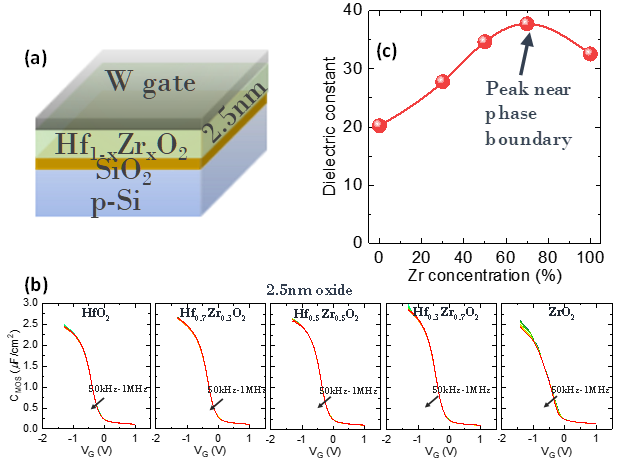
An example of the ultrathin ALD grown HZO device displaying dielectric constant enhancement at the morphotropic phase boundary is shown in Figure 1.

Figure 1: (a) Schematic of the ultrathin HZO MOSCAP devices and corresponding (b) capacitance-voltage (C-V) curves for different Zr concentrations. (c) Dielectric constant extraction from thickness dependent C-V as a function of Zr concentration highlighting the dielectric constant boost at the proposed morphotropic phase boundary near 70% Zr. (Ref. 1).

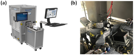
Figure 2: (a) Kurt J. Lesker Company model ALD-150LX with full software control and (b) in-situ ellipsometer mounted to the process chamber.
The films were grown using a Kurt J. Lesker Company ALD-150LX atomic layer deposition (ALD) system equipped with a high vacuum load lock, 150mm wafer handling capability and integrated FS-1 in-situ ellipsometry for real-time film thickness monitoring. The ALD-150LX has substrate heating capability to 500°C, vapor draw and flow-through source delivery with independent input lines and remote inductive plasma capability utilizing ultra-high purity gases such as Ar, O2, O3, N2, H2 and NH3 for deposition of high-quality oxides and nitrides.

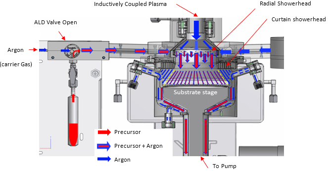
Figure 3: Lesker ALD shower head with patented precursor focusing technique (PFTTM) (Ref 3).
References:
1. K. Ni et al., "Equivalent Oxide Thickness (EOT) Scaling With Hafnium Zirconium Oxide High-K Dielectric Near Morphotropic Phase Boundary", International Electronic Devices Meeting (IEDM) (2019); doi: https://doi.org/10.1109/IEDM19573.2019.8993495
2. S. Cheema et al., "Enhanced ferroelectricity in ultrathin films grown directly on silicon", Nature (2020); https://doi.org/10.1038/s41586-020-2208-x
3. G. B. Rayner, Jr., U.S. Patent No. 9,695,510, "Atomic Layer Deposition Apparatus and Process" (2017).


