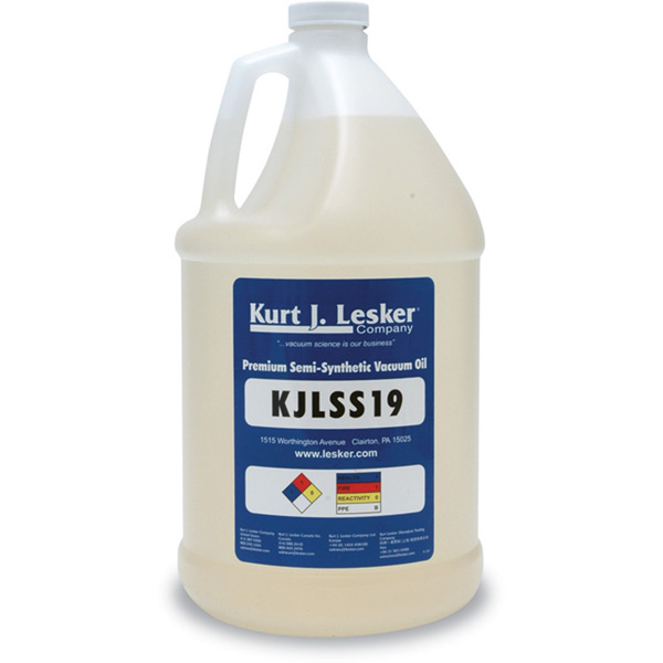
KJLC's new line of semi-synthetic mechanical pump oils offers superior performance. KJLSS oil contains an anti-oxidation additive which extends the useful life of the oil. With its low vapor pressure this oil is an ideal choice for a variety of applications. KJLSS is a semi-synthetic oil with a high viscosity index, which makes it much more energy efficient than many other vacuum pump oils. It has the added benefit of being able to withstand higher operating temperatures. This new oil is available in four different types, with varying viscosities.
Features
- Food Industry Approved — NSF H2
- High viscosity index
- Greater energy efficiency
- Superior resistance to high temperatures
- Increased oxidation resistance
- Operates at extremely low vapor pressures
Benefits
- Extended lubrication life
- Increases pump reliability, efficiency, and life expectancy
- Extended interval between oil changes
Specifications Table
| Property | |||
|---|---|---|---|
| Vapor Pressure mm Hg @ 25°C | |||
| Pour Point | |||
| Flash Point | |||
| Viscosity @ 40°C | |||
| Viscosity Index | |||
| Corrosion Protection: Rust A - Distilled Water Rust B - Synthetic Sea Water | |||
| Rotary Pressure Vessel Oxidation Test, minutes |
Shelf Life
It is strongly recommended using all fluids and greases at the time of receipt, however when storage is necessary, rotate older stock into use first and observe the recommended parameters listed below.
Hydrocarbon Oils
The hydrocarbon oil products do not have an expiration date specified. The longevity of products shipped is based primarily on the storage and handling conditions after the product leaves the control of the Kurt J Lesker Company. Limited laboratory testing indicates that all products will last more than three years from the date of shipment, if unopened and stored in a dry and dark environment at a temperature range of 60F-85F (15-30C). It is up to the individual customer to evaluate the longevity (expiration date) of the product based on their particular storage and handling conditions.


