May 25, 2022 | By KJLC Blog
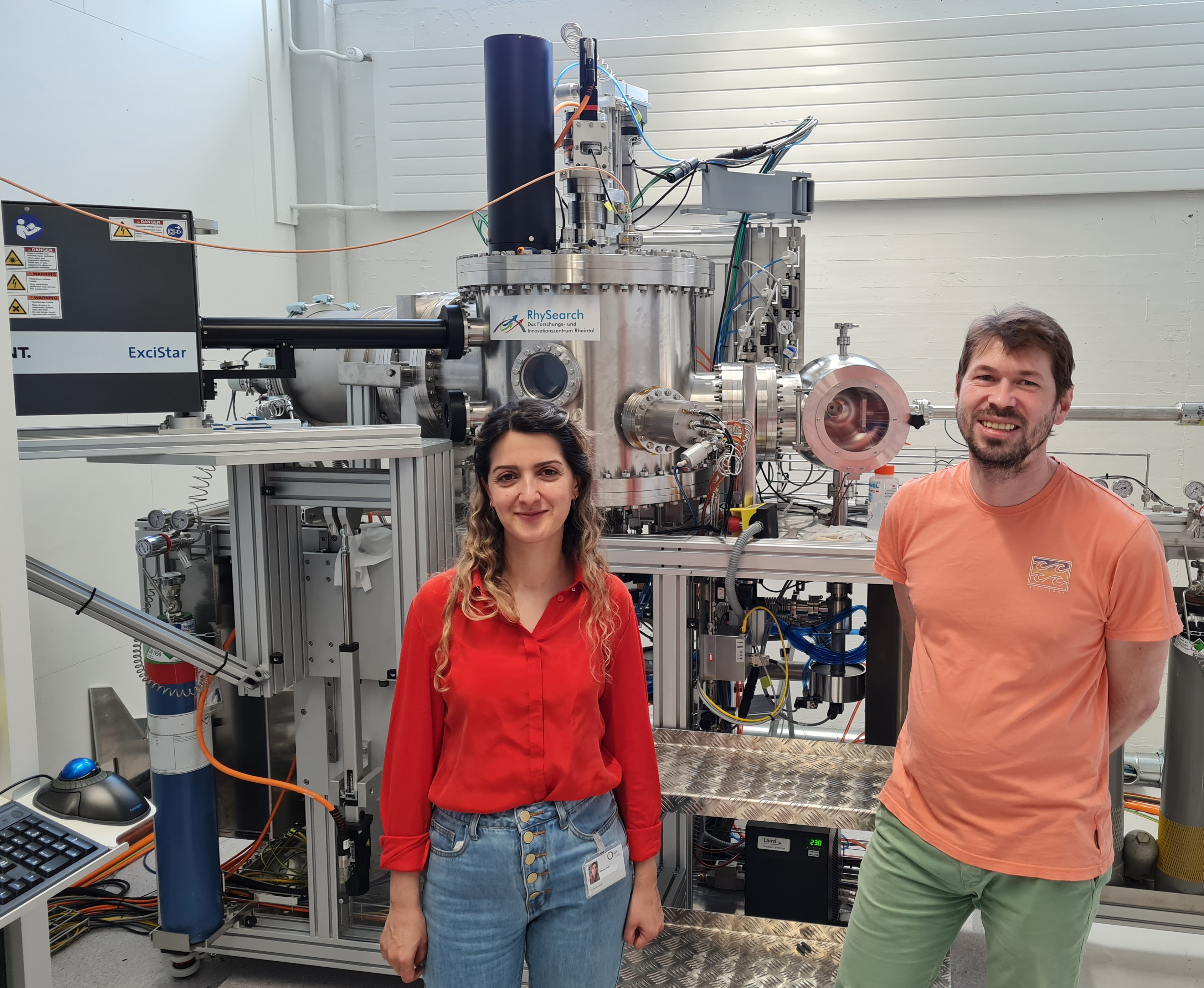
We are proud to have supported our customer RhySearch in Switzerland with equipment for their Ion Beam Sputtering of 2D Materials project.For this project, we supported RhySearch with the design and manufacturing of the complete vacuum system. The core of the project is the UHV vacuum chamber, which was manufactured and delivered by the Kurt J. Lesker Company. We also supplied most of the relevant equipment around the vacuum chamber, including motion manipulation parts, vacuum pumps, gauges, feedthroughs and valves.
Read More
Tags:
Systems
Vacuum Science
Deposition Techniques
January 17, 2022 | By KJLC Innovate
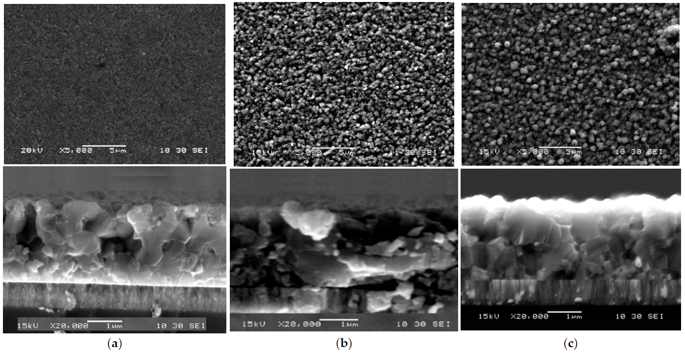
The Kurt J Lesker Company has been providing Physical Vapor Deposition (PVD) systems to support photovoltaics (PV) research for more than 20 years and continues to support scientists globally to advance this critical renewable energy application. Solar cells work by using materials that absorb photons from sunlight in a broad spectral range and in turn effectively convert this captured light into free charges that produce electricity. Modern commercial solar cells are mainly based on crystalline Silicon, which is a cheap and abundant semiconductor[1]. In recent decades, alternative thin film technologies based on materials combinations including Copper indium gallium diselenide (Cu(In,Ga)Se2 or CIGS), Cadmium Telluride (CdTe), amorphous silicon and organic photovoltaics (OPV) have emerged with high efficiencies coupled with good cell stability, low manufacturing costs and come with the advantage of being a thin film, being both lightweight and flexible[2].
Read More
Tags:
INNOVATE
Systems
Vacuum Science
Deposition Techniques
December 01, 2021 | By KJLC Innovate
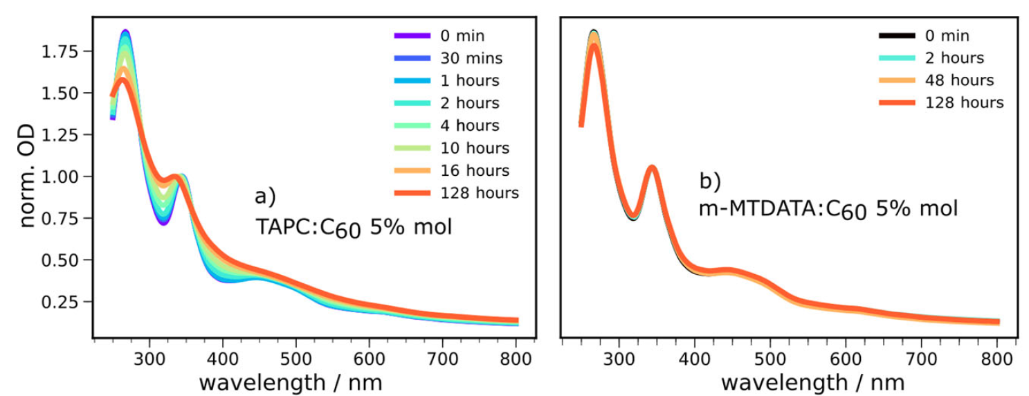
Organic electronics research has advanced rapidly over the past few decades, with organic light-emitting diodes (OLEDs) now being commonly available in commercial devices such as mobile phones and TVs. Organic photovoltaics (OPVs, or organic solar cells) have potential to follow OLEDs as a commercially viable technology, but a number of challenges still need to be overcome. A recent publication from an international collaboration, with lead authors Prof. Moritz Riede (University of Oxford) and Dr. Ivan Ramirez (Heliatek GmbH), has investigated the degradation pathways of OPV devices using a common organic material, C60, generating understanding which may prove critical to achieve long-term device stability. The complete solar cell structures used in the study were produced using a Kurt J. Lesker SPECTROS evaporation system.
Read More
Tags:
INNOVATE
Systems
Vacuum Science
Deposition Techniques
October 13, 2021 | By KJLC Innovate
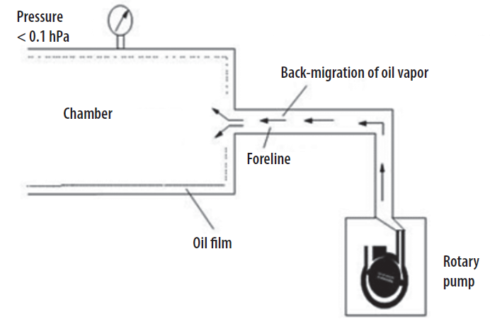
Systems evacuated with oil-based pumps may be victims of backstreaming of pump oil vapors into the fore- line, vacuum chamber, and upstream throughout the system. The back- streaming referred to here is the act of pump oil vapors moving against the flow of molecules traveling from the vacuum chamber to the pump(s). In this case, we refer to these oil vapors as moving upstream, and eventually into the vacuum chamber. At high pressures, where the number of molecules from the chamber outnumber pump oil vapor molecules emanating from the pumping system, flow upstream is greatly mitigated. Oil vapor back- streaming is significantly more pronounced at lower operating pressures.
Read More
Tags:
INNOVATE
Systems
Vacuum Science
Deposition Techniques
June 07, 2021 | By KJLC Innovate
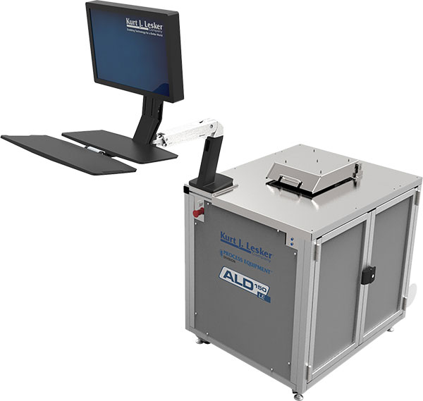
Mina Shahmohammadi from the research group of Professor Christos G. Takoudis, Full Professor in the Departments of Bioengineering and Chemical Engineering at the University of Illinois at Chicago, in collaboration with College of Dentistry, University of Illinois at Chicago, and Kurt J. Lesker Company recently developed conformal atomic layer deposition (ALD) based titanium (IV) oxide (TiO2) thin film processes on Polymethyl Methacrylate (PMMA) displaying excellent surface and mechanical properties for potential engineering, medical, and biomedical applications. The findings were recently published in the Journal of Materials Science.
Read More
Tags:
INNOVATE
Systems
Vacuum Science
Deposition Techniques
April 19, 2021 | By KJLC Innovate
 *Photo: ISFH, taken by Salzmann-Fotografie*
The Kurt J Lesker Company has been shipping Physical Vapor Deposition (PVD) tools into the field of perovskite solar cells for the last decade and continues to support researchers in this exciting application. Our partner, Dr. Sascha J. Wolter, along with the Future Technologies Photovoltaics group, headed by Dr. Sarah Kajari-Schröder, at the Institute for Solar Energy Research (ISFH) in Hamelin, Germany, have presented a method to determine the acoustic impedance ratio (Z) for two perovskite precursors that are commonly co-deposited using PVD. In their paper "Determination and influence evaluation of the acoustic impedance ratio for thermal evaporation"[1] they report Z values for methylammonium iodide (MAI) of 0.025 ±0.002 and 0.11 ±0.01 for lead (II) iodide (PbI2). Furthermore, the impact of using an incorrect Z-ratio on actual experimental thermal evaporations is investigated.
Read More
Tags:
INNOVATE
Systems
Vacuum Science
Deposition Techniques
March 04, 2021 | By KJLC Innovate

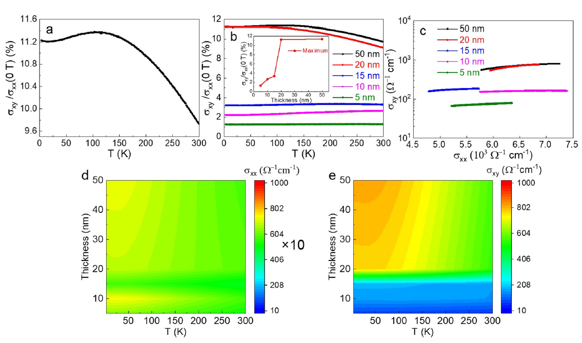
When a magnetic field (B in Fig. 1 (a)) is applied to a metal, the electric current (J in Fig. 1 (a)) flowing through the metal will be deflected by the magnetic field so that it is not parallel with the applied electric field (E in Fig. 1 (a)). This phenomenon, known as the Hall effect, is well understood in the classical physics. Later, the research on magnetic materials discovered that in certain magnetic materials, the Berry phase, one of the quantum properties of electrons, can alter the motion of electrons without the presence of an external magnetic field (Fig. 1 (b)). This phenomenon is known as the anomalous Hall effect (AHE). In AHE experiments, two quantities are measured: The longitudinal conductivity σxx, which is the conductivity of the material along the direction of the electric field; and the transverse conductivity σxy, which is the conductivity along the perpendicular direction of the electric field. The ratio between σxy and σxx, defined as the anomalous Hall angle, measures the strength of the intrinsic deflection by the Berry phase: The higher the σxy/σxx is, the more prominent the Berry phase is.
Read More
Tags:
INNOVATE
Systems
Vacuum Science
Deposition Techniques
January 29, 2021 | By KJLC Innovate
The Kurt J. Lesker Company (KJLC) has supported organic electronics research since producing its first dedicated PVD tool series over 20 years ago, enabling many breakthrough results. Recently a team from CNR NANOTEC (Lecce, Italy) has reported a strategy to improve the stability and durability of flexible top-emitting organic light-emitting diodes in their paper "Flexible distributed Bragg reflectors as optical outcouplers for OLEDs based on a polymeric anode", with results obtained using both KJLC deposition tools and materials.
Read More
Tags:
INNOVATE
Systems
Vacuum Science
Deposition Techniques
January 29, 2021 | By KJLC Innovate

The ability to fabricate flexible nano-thin films is of great interest because of the increased demand for flexible technologies, a paradigm shift in high-tech and consumer electronics, already making significant technological and commercial impact by enabling the emergence of flexible photovoltaics, flexible electronics, flexible smart textiles and flexible displays. Flexible thin films are typically achieved by coating a given material onto a flexible substrate, via a chemical vapour deposition (CVD) process, where the coating ingredients are mostly organic materials and chemicals. Coating flexible thin films from inorganic materials such as metals, functional alloys, heterostructures, semiconductors, oxides and ceramics via solid state DC / RF plasma sputtering is less known, and it is unclear how the flexible substrate affects their properties. This project demonstrated the successful production of flexible magnetic thin films with excellent adhesion and mechanical robustness. Remarkably, the films maintained their structure, integrity and physical properties at any curvature bending applied to the flexible samples.
Read More
Tags:
INNOVATE
Systems
Vacuum Science
Deposition Techniques
January 21, 2021 | By KJLC Innovate
Electrons have two fundamental physical properties, their charge and spin. The charge of electrons has been discovered and carefully measured long time ago[1]. The utilization of the electron charge can be found in all electronic devices. The manipulation of the electron spin, on the other hand, has been proved to be more challenging because of its quantum mechanical nature. To elucidate the physics and to design applications of the electron spin, a research area named spintronics has been established, and its rapid advance has identified the essential role of the electron spin in many fundamental properties of condensed matter systems such as the spin Hall effect[2] and the quantum spin Hall effect[3]. In addition, the research on the electron spin has resulted in numerous applications such as the giant magnetoresistance structures and tunneling magnetoresistance devices[4].
Read More
Tags:
INNOVATE
Systems
Vacuum Science
Deposition Techniques
Previous Entries
Next Entries
