Semiconductor Quantum Wires (QW) are nanoscale structures of semiconductor material whose electro-optical properties are heavily influenced by electron quantum confinement effects, due to their small structure. These structures show great promise for use in applications including sensors, quantum computing, bioelectronic and solar cells [1, 2, 3]. It is stated that, traditionally, 3D structures of QW are fabricated using high-resolution lithography. This is a very complex and expensive method making it less appealing for large scale production of QW devices. A team at the Rudjer Boskovic Institute in Croatia, in collaboration with the National Institute of Chemistry (Ljubljana) and the Slovak Academy of Sciences developed a simple method for tuning the parameters of the QW lattice unit cell by depositing self-assembling Germanium (Ge) QW in an Alumina (Al2O3) matrix by co-sputtering [4]. This straightforward approach involves varying the Ge DC sputtering power, in order to control the Ge concentration in the matrix, and the temperature of the substrate during the deposition.
This research concludes that the QW network will adjust its own parameters (i.e. tilt angle and QW length) to incorporate the additional Ge in the sputtering process.
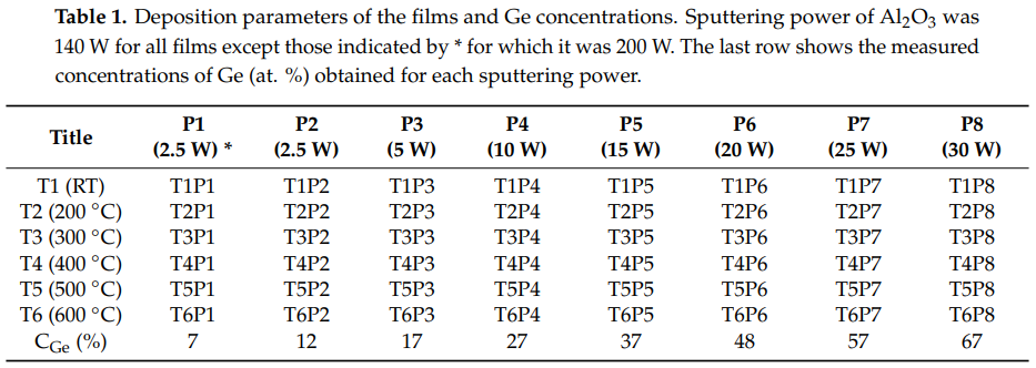
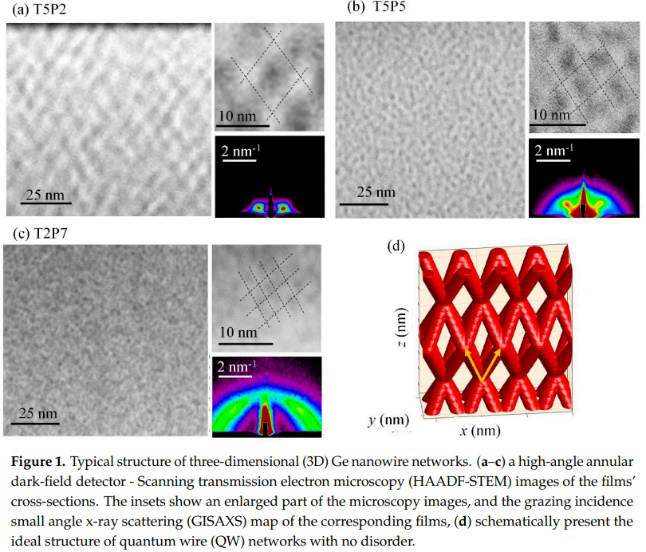
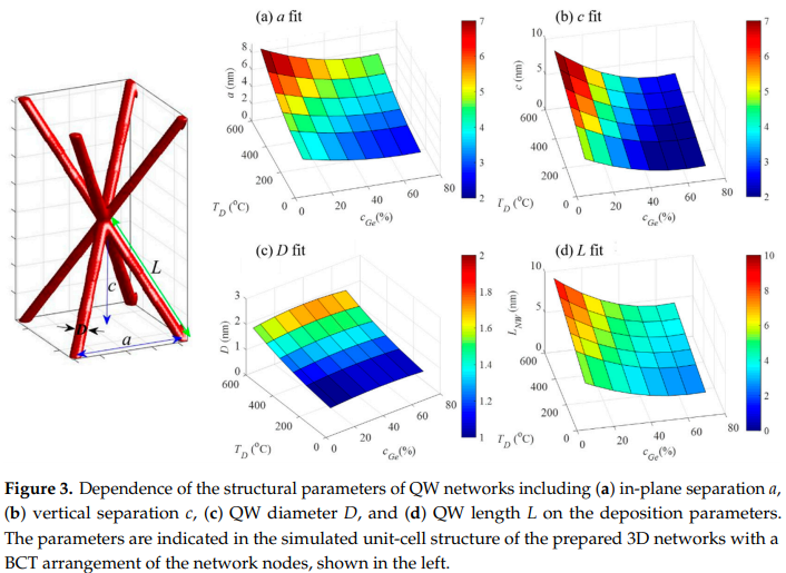
Sputtering power and substrate temperature are varied and the resulting networks of QWs are measured using STEM imaging and Grazing Incidence small angle x-ray scattering (GISAXS). GISAXS uses the diffraction pattern of scattered x-rays measured in a 2D array to determine geometrical properties of 3D nanostructure [5, 6] present in the film. Small, narrow Bragg spots indicate a well separated and highly ordered QW structure [7], as can be seen in the T5P2 film. Less ordering and large, diffuse Bragg spots indicate and narrow and poorly ordered structure such as that in the T2P7 film.
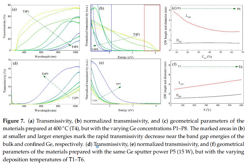
Controlling the QW unit cell parameters is key to tuning their opto-electrical properties, namely the transmittivity of the bulk material. Typically, reducing the length of the QWs increases the quantum confinement effects imposed on the electrons, thus increasing the band gap of the material and increasing the energy at which the transmittance goes to zero. The results displayed in this research show the opposite trend to these assumptions; increasing the Ge concentration reduces the transmittance cut-off energy. It is hypothesised that this comes as a result of increased radius of the Ge structure at the nodes where 8 QWs meet. This region can then no longer be treated as a simple wire but must be considered as a more complex 3D shape. As there are a much higher number of these nodes in the higher Ge concentration films the contribution of these nodes is higher and the transmittance spectrum is heavily affected.
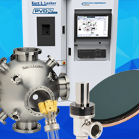
The research presented was conducted in a Kurt J Lesker CMS-18 (https://www.lesker.com/newweb/vacuum_systems/deposition_systems_pvd_cms18.cfm) using high purity Ge (99.999%) and Al2O3 (99.999%) supplied by the KJLC. This system consists of a 4 sputter gun baseplate system equipped with 4 3-inch TORUS sputter guns, both with high and standard strength magnet assemblies and capable of both RF and DC sputtering as well as a 600°C substrate heater.
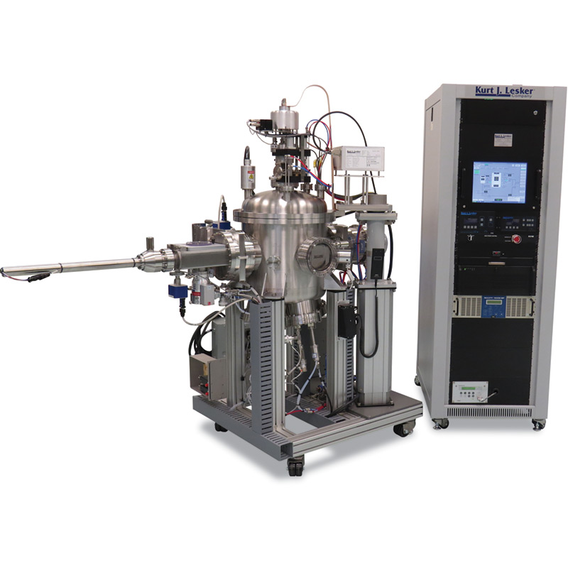
The system offers rigid repeatability with high precision closed loop control all process components, from sputter power to substrate heating. This provides accurate comparisons between process runs due to the confidence in the consistency of the deposition conditions. The extremely low base pressures the system offers ensures the composition of the films is dependable and predictable further improving the run to run comparability.
References
- Tian, Bozhi, et al., "Coaxial silicon nanowires as solar cells and nanoelectronic power sources.," nature, vol. 449.7164, pp. 885-889, 2007.
- Garnett, Erik C, et al., "Nanowire solar cells.," Annual Review of Materials Research, vol. 41, pp. 269-295., 2011.
- Zhou W, Dai X, Lieber CM., "Advances in nanowire bioelectronics.," Reports on Progress in Physics, vol. 80.1, p. 016701, 2016.
- Basioli, Lovro, et al., "3D Networks of Ge Quantum Wires in Amorphous Alumina Matrix," Nanomaterials, vol. 10.7, p. 1363, 2020.
- Rauber, Markus, et al., "Highly-ordered supportless three-dimensional nanowire networks with tunable complexity and interwire connectivity for device integration.," Nano letters, vol. 11.6, pp. 2304-2310, 2011.
- Ray, Nirat, et al., "Influence of Structure on Electronic Charge Transport in 3D Ge Nanowire Networks in an Alumina Matrix.," Scientific reports, vol. 9.1, pp. 1-9, 2019.
- Basioli, Lovro, et al., "Application of GISAXS in the Investigation of Three-Dimensional Lattices of Nanostructures.," Crystals, vol. 9.9, p. 479, 2019.
