January 29, 2021 | By KJLC Innovate
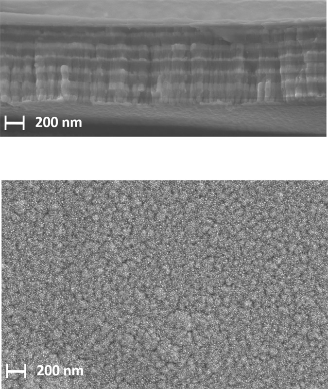
The Kurt J. Lesker Company (KJLC) has supported organic electronics research since producing its first dedicated PVD tool series over 20 years ago, enabling many breakthrough results. Recently a team from CNR NANOTEC (Lecce, Italy) has reported a strategy to improve the stability and durability of flexible top-emitting organic light-emitting diodes in their paper "Flexible distributed Bragg reflectors as optical outcouplers for OLEDs based on a polymeric anode", with results obtained using both KJLC deposition tools and materials.
Read More
Tags:
INNOVATE
Systems
Vacuum Science
Deposition Techniques
January 29, 2021 | By KJLC Innovate

The ability to fabricate flexible nano-thin films is of great interest because of the increased demand for flexible technologies, a paradigm shift in high-tech and consumer electronics, already making significant technological and commercial impact by enabling the emergence of flexible photovoltaics, flexible electronics, flexible smart textiles and flexible displays. Flexible thin films are typically achieved by coating a given material onto a flexible substrate, via a chemical vapour deposition (CVD) process, where the coating ingredients are mostly organic materials and chemicals. Coating flexible thin films from inorganic materials such as metals, functional alloys, heterostructures, semiconductors, oxides and ceramics via solid state DC / RF plasma sputtering is less known, and it is unclear how the flexible substrate affects their properties. This project demonstrated the successful production of flexible magnetic thin films with excellent adhesion and mechanical robustness. Remarkably, the films maintained their structure, integrity and physical properties at any curvature bending applied to the flexible samples.
Read More
Tags:
INNOVATE
Systems
Vacuum Science
Deposition Techniques
January 21, 2021 | By KJLC Innovate
Electrons have two fundamental physical properties, their charge and spin. The charge of electrons has been discovered and carefully measured long time ago[1]. The utilization of the electron charge can be found in all electronic devices. The manipulation of the electron spin, on the other hand, has been proved to be more challenging because of its quantum mechanical nature. To elucidate the physics and to design applications of the electron spin, a research area named spintronics has been established, and its rapid advance has identified the essential role of the electron spin in many fundamental properties of condensed matter systems such as the spin Hall effect[2] and the quantum spin Hall effect[3]. In addition, the research on the electron spin has resulted in numerous applications such as the giant magnetoresistance structures and tunneling magnetoresistance devices[4].
Read More
Tags:
INNOVATE
Systems
Vacuum Science
Deposition Techniques
January 20, 2021 | By KJLC Innovate

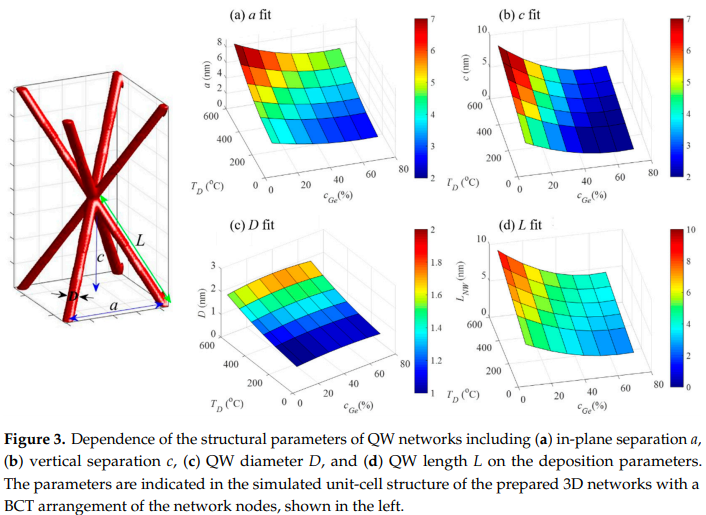
Semiconductor Quantum Wires (QW) are nanoscale structures of semiconductor material whose electro-optical properties are heavily influenced by electron quantum confinement effects, due to their small structure. These structures show great promise for use in applications including sensors, quantum computing, bioelectronic and solar cells [1, 2, 3]. It is stated that, traditionally, 3D structures of QW are fabricated using high-resolution lithography. This is a very complex and expensive method making it less appealing for large scale production of QW devices. A team at the Rudjer Boskovic Institute in Croatia, in collaboration with the National Institute of Chemistry (Ljubljana) and the Slovak Academy of Sciences developed a simple method for tuning the parameters of the QW lattice unit cell by depositing self-assembling Germanium (Ge) QW in an Alumina (Al2O3) matrix by co-sputtering [4]. This straightforward approach involves varying the Ge DC sputtering power, in order to control the Ge concentration in the matrix, and the temperature of the substrate during the deposition.
Read More
Tags:
INNOVATE
Systems
Vacuum Science
Deposition Techniques
January 11, 2021 | By KJLC Innovate
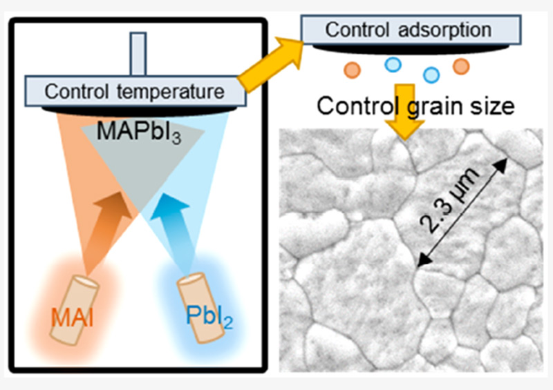
For nearly a decade the Kurt J Lesker Company has been shipping Physical Vapor Deposition (PVD) tools into the field of perovskite solar cells around the world and continues to support world class research into this exciting technology. A key topic in the fabrication of vapor deposited perovskite photovoltaics is how much the crystal grain boundaries affect the solar cell performance (see Figure 1). Recent work, published in ACS Energy Letters, titled "Control over crystal size in vapor deposited metal-halide perovskite films' by Killian Lohmann, Jay Patel, Mathias Uller Rothmann, Chelsea Xia, Robert Oliver, Laura Herz, Henry Snaith and Michael Johnston from the University of Oxford, in the UK, has not only identified key parameters that effect the grain growth in perovskite thin films but the team has also developed a novel method to control the deposition of the organic precursor, resulting in highly efficient solar cells.
Read More
Tags:
INNOVATE
Systems
Vacuum Science
Deposition Techniques
October 26, 2020 | By KJLC Innovate
The Kurt J. Lesker Company continues to support the researchers who are advancing the science and technology of spintronics around the world. Co2MnGa, a Heusler material, has been attractive to scientists as a novel magnetic conducting material on which spintronic structures like magnetic tunnel junctions can be built. Recent work, published in Applied Physics Letter titled "Perpendicular magnetic anisotropy in Co2MnGa and its anomalous Hall Effect" by Dr. Ludbrook, Dr. Ruck and Dr. Granville from Victoria University of Wellington, New Zealand, has identified characteristics of thin film Co2MnGa that are necessary for realizing magnetic tunnel junctions.
Read More
Tags:
INNOVATE
Systems
Vacuum Science
Deposition Techniques
October 01, 2020 | By KJLC Innovate

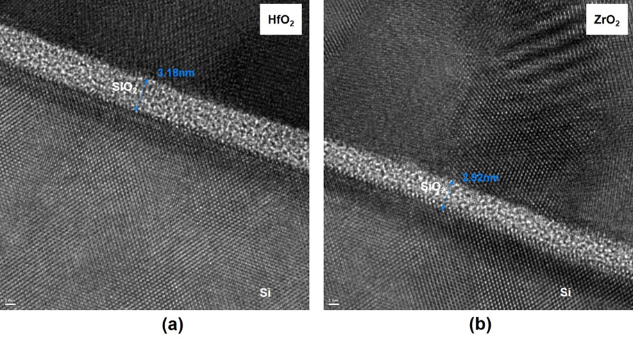
Dr. Zhigang Xiao, Professor of Electrical Engineering at Alabama A&M University, in collaboration with the ALD group in the Kurt J. Lesker Company recently developed the plasma-enhanced atomic layer deposition process and grow high dielectric constant (K) oxide for the application of electronic materials. They grew nanoscale hafnium dioxide (HfO2) and zirconium dioxide (ZrO2) thin films using remote plasma-enhanced atomic layer deposition (PE-ALD) and fabricated complementary metal-oxide semiconductor (CMOS) integrated circuits using the HfO2 and ZrO2 thin films as the gate oxide. Miniaturization in modern semiconductor industry requires thin film deposition to have atomic level control and the deposited film to be conformal and pinhole-free. As MOSFETs are scaled down to nanometer sizes, the tunneling currents through the gate dielectrics (the gate leakage current) has become a major concern in today’s fabrication of integrated circuits (ICs). High-K dielectric metal oxide could be a solution to the problem of the gate leakage current. The plasma-enhanced atomic layer deposition of HfO2 and ZrO2 thin films meets the requirement and can produce conformal and ultra-thin films with precise thickness control at the atomic layer level. The experimental results measured from the HfO2 and ZrO2 thin films were compared.
Read More
Tags:
INNOVATE
Systems
Vacuum Science
Deposition Techniques
June 01, 2020 | By KJLC Innovate

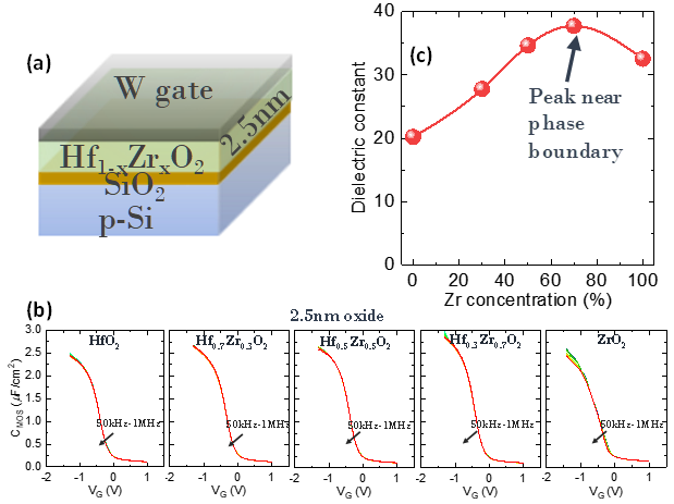
Dr. Kai Ni from the research group of Professor Suman Datta, Stinson Professor of Nanotechnology at the University of Notre Dame, in collaboration with Purdue University and Kurt J. Lesker Company recently developed conformal atomic layer deposition (ALD) based hafnium zirconium oxide thin film processes displaying excellent electrical properties for potential gate oxide complement or replacement in scaled logic and memory technology nodes. The findings were recently published and showcased in the IEEE International Electron Devices Meeting (IEDM) 2019 in San Francisco, CA [ref. 1]. In particular, hafnium zirconium oxide (HfxZr1-xO2, or HZO) has emerged as a ferroelectric (large charge density per unit area) material system that also displays a tunable permittivity or dielectric constant (charge response) depending on the concentration of Zr added to the base HfO2 oxide. The reported films indicate that by sweeping the concentration of Zr in HfO2 during the ALD growth, a substantial boost in the dielectric constant can be observed around 70% Zr concentration due to the presence of a crystallographic phase transition of the underlying HZO material structure, which results in enhanced electrical performance even in ultrathin films 25Å thick [ref. 2]. These findings elucidate the necessity and importance of extremely stringent deposition process control along with corresponding electrical and structural characterization for the understanding of new materials systems for their further implementation in commercial applications such as high-performance digital and analog CMOS technology at advanced nodes.
Read More
Tags:
INNOVATE
Systems
Vacuum Science
Deposition Techniques
May 01, 2020 | By KJLC Blog

In a recently issued patent (US 10,619,950 April 14, 2020) researchers at the Toyota Motor Company have demonstrated that the corrosion resistance of stainless steel exhaust systems for cars and trucks can be substantially improved by heat treatment in high vacuum. Stainless steel is a complex metal alloy of iron, nickel, chrome and other elements. It is known to be a very durable metal but even this robust material can be corroded by exposure to chloride ions, sulfuric and hydrochloric acids, soot and other artifacts of the exhaust from an internal combustion engine. Reaction with these aggressive gases causes pits in steel which eventually lead to premature failure. The use of low-grade fuels speeds the degradation of exhaust systems.
Read More
Tags:
INNOVATE
Systems
Vacuum Science
Deposition Techniques
March 06, 2020 | By KJLC Innovate

Dr. Nicholas A. Strnad (General Technical Services, LLC) in collaboration with the U.S. Army Combat Capabilities Command Army Research Laboratory and the University of Maryland, College Park have recently developed conformal processes for a variety of lead-based electronic materials with outstanding properties using atomic layer deposition (ALD)...
Read More
Tags:
INNOVATE
Systems
Vacuum Science
Deposition Techniques
Previous Entries
Next Entries
