January 21, 2021 | By KJLC Innovate
Electrons have two fundamental physical properties, their charge and spin. The charge of electrons has been discovered and carefully measured long time ago[1]. The utilization of the electron charge can be found in all electronic devices. The manipulation of the electron spin, on the other hand, has been proved to be more challenging because of its quantum mechanical nature. To elucidate the physics and to design applications of the electron spin, a research area named spintronics has been established, and its rapid advance has identified the essential role of the electron spin in many fundamental properties of condensed matter systems such as the spin Hall effect[2] and the quantum spin Hall effect[3]. In addition, the research on the electron spin has resulted in numerous applications such as the giant magnetoresistance structures and tunneling magnetoresistance devices[4].
Read More
Tags:
INNOVATE
Systems
Vacuum Science
Deposition Techniques
January 20, 2021 | By KJLC Innovate

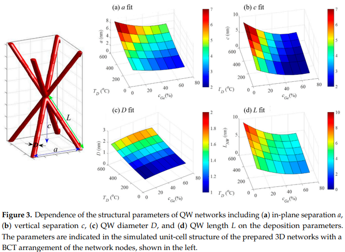
Semiconductor Quantum Wires (QW) are nanoscale structures of semiconductor material whose electro-optical properties are heavily influenced by electron quantum confinement effects, due to their small structure. These structures show great promise for use in applications including sensors, quantum computing, bioelectronic and solar cells [1, 2, 3]. It is stated that, traditionally, 3D structures of QW are fabricated using high-resolution lithography. This is a very complex and expensive method making it less appealing for large scale production of QW devices. A team at the Rudjer Boskovic Institute in Croatia, in collaboration with the National Institute of Chemistry (Ljubljana) and the Slovak Academy of Sciences developed a simple method for tuning the parameters of the QW lattice unit cell by depositing self-assembling Germanium (Ge) QW in an Alumina (Al2O3) matrix by co-sputtering [4]. This straightforward approach involves varying the Ge DC sputtering power, in order to control the Ge concentration in the matrix, and the temperature of the substrate during the deposition.
Read More
Tags:
INNOVATE
Systems
Vacuum Science
Deposition Techniques
January 11, 2021 | By KJLC Innovate
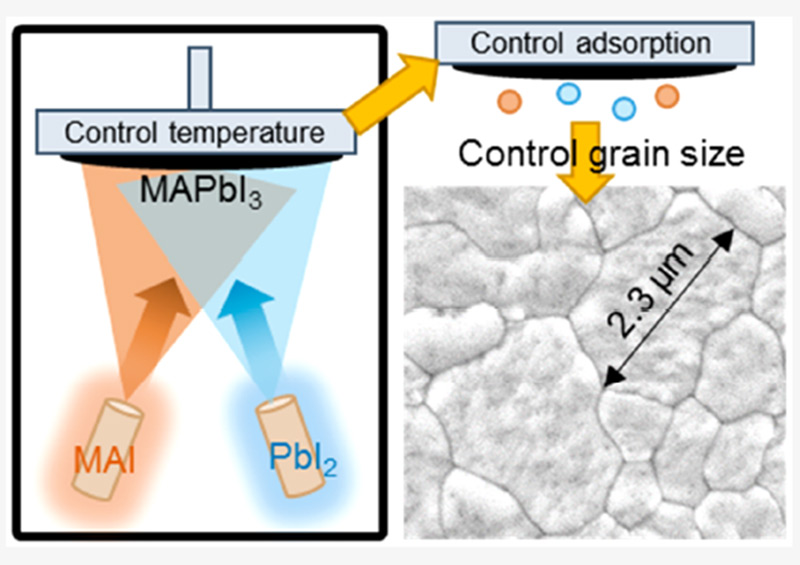
For nearly a decade the Kurt J Lesker Company has been shipping Physical Vapor Deposition (PVD) tools into the field of perovskite solar cells around the world and continues to support world class research into this exciting technology. A key topic in the fabrication of vapor deposited perovskite photovoltaics is how much the crystal grain boundaries affect the solar cell performance (see Figure 1). Recent work, published in ACS Energy Letters, titled "Control over crystal size in vapor deposited metal-halide perovskite films' by Killian Lohmann, Jay Patel, Mathias Uller Rothmann, Chelsea Xia, Robert Oliver, Laura Herz, Henry Snaith and Michael Johnston from the University of Oxford, in the UK, has not only identified key parameters that effect the grain growth in perovskite thin films but the team has also developed a novel method to control the deposition of the organic precursor, resulting in highly efficient solar cells.
Read More
Tags:
INNOVATE
Systems
Vacuum Science
Deposition Techniques
Next Entries
