July 29, 2015 | By KJLC Innovate

Plasmonics is an important field of research with applications in bio-sensing, photocatalysis, solar cells and high-speed computing, among others. The fundamental technologically enabling features of plasmonics are sub-wavelength confinement of electromagnetic fields and ultra-strong enhancement of those fields. Highly-reflective metals are the predominant material choice for plasmonic devices. More specifically, Gold and Silver have been the most studied materials to date. Aluminum and Copper are burgeoning plasmonic materials which offer CMOS compatibility and low cost. Furthermore, Aluminium opens up the possibility of ultraviolet plasmonic devices which have recently been shown to have applications in bio-sensing and colour filters.
Read More
Tags:
INNOVATE
Systems
Vacuum Science
March 30, 2015 | By KJLC Innovate

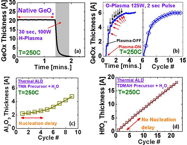
Germanium (Ge) is a promising candidate to enhance p-channel metal oxide silicon field transistor (MOSFET) device performance. The successful development of Ge-based field effect devices requires the integration of a high-quality dielectric with equivalent oxide thickness (EOT) less than 1 nanometer that forms an electrically well behaved semiconductor dielectric interface. Although GeOx/Ge has been found promising, the thermodynamic instability as well as the relatively low dielectric constant of GeOx requires an alternative approach. The utilization of an ultrathin Si layer, to modify the semiconductor-dielectric interface from Ge into Si, is a viable approach that has been successfully demonstrated; however, the introduction of a thin Si layer into the gate stack is incompatible with the 3D FinFET manufacturing process flow and also leads to increased EOT. It is, therefore, desirable to develop a multilayer gate-stack by atomic layer deposition (ALD), where an ultrathin GeOx layer can be thermodynamically stabilized and combined with a high-k dielectric film to meet the stringent requirement of low interface trap density and large capacitance density while maintaining a low gate leakage under the constraint of full compatibility with modern 3D FinFET geometries.
Read More
Tags:
INNOVATE
Systems
Vacuum Science
March 25, 2015 | By KJLC Innovate

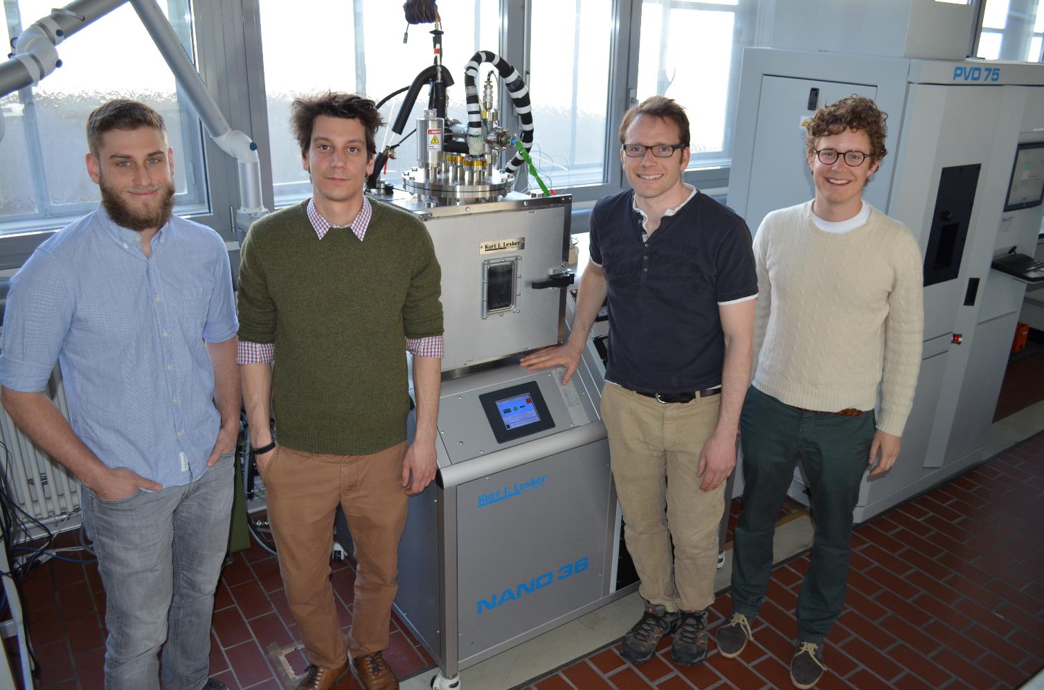
Kurt J. Lesker Company and Penn State University have jointly developed a multi-technique process tool enabling high-k metal gate development for high mobility channel transistor technology.
The dual process chamber design allows preparation of pristine semiconductor surfaces and their passivation (UHV-MBE), while the PEALD system provides state-of-the-art high-k deposition capabilities. Both process chambers are equipped with analytical ports for in-situ process monitoring and control by spectroscopic ellipsometry (SE).
Read More
Tags:
INNOVATE
Systems
Vacuum Science
