The Kurt J Lesker Company has been providing Physical Vapor Deposition (PVD) systems to support photovoltaics (PV) research for more than 20 years and continues to support scientists globally to advance this critical renewable energy application. Solar cells work by using materials that absorb photons from sunlight in a broad spectral range and in turn effectively convert this captured light into free charges that produce electricity. Modern commercial solar cells are mainly based on crystalline Silicon, which is a cheap and abundant semiconductor[1]. In recent decades, alternative thin film technologies based on materials combinations including Copper indium gallium diselenide (Cu(In,Ga)Se2 or CIGS), Cadmium Telluride (CdTe), amorphous silicon and organic photovoltaics (OPV) have emerged with high efficiencies coupled with good cell stability, low manufacturing costs and come with the advantage of being a thin film, being both lightweight and flexible[2].
CIGS based solar cells are one of the most successful thin film photovoltaic technologies that currently exist[3], and vacuum-processing is one of the most common methods to achieve highly repeatable and efficient CIGS PV devices[4]. Our partner, Dr. Sylvain Marsillac from the Virginia Institute of Photovoltaics at Old Dominion University in Norfolk, Virginia, US, along with a team from Old Dominion University, the Colorado School of Mines, US and the University of Nantes, France have investigated the influence of the deposition parameters on the in-situ recrystallization via a CuCl2 vapor of CIGS thin films deposited by a modified three-stage co-evaporation process at low temperatures and high deposition rates. In their paper “In Situ Recrystallization of Co-Evaporated Cu(In,Ga)Se2 Thin Films by Copper Chloride Vapor Treatment towards Solar Cell Applications”[5] they report on the performance of the CIGS films and solar cell devices, fabricated at low temperatures and high deposition rates as, a function of varying deposition parameters.
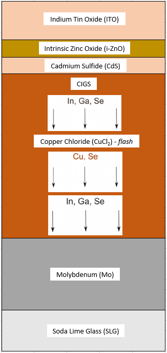
CIGS absorber layers with large grain sizes and high crystallinity, deposited at low substrate temperatures are essential to the development of CIGS solar cells. These cells are typically fabricated using a three-stage co-evaporation process[6]. During this process, In, Ga, and Se are evaporated in the 1st and 3rd stage while Cu and Se are deposited in-between. Solar cells with power conversion efficiencies >23% have been obtained with this method, however this process uses high substrate temperatures up to 550°C, which lead to such cells lagging existing crystalline silicon solar cells in terms of their economic viability. As a result, there has been a drive to improve the cost competitiveness of CIGS by reducing fabrication times by leveraging low processing temperatures coupled with high deposition rates. The group at Old Dominion fabricated CIGS devices via this three-stage process with high deposition rates (~10µm/hr) with a constant first stage temperature, but with a varying (low and high) second and third stage temperatures - with an in-situ CuCl2 vapor treatment in between the second and third stages. This modified, third stage, has resulted in the selective enhancement of some properties in CIGS PV cells. The overall process is shown in Figure 1.
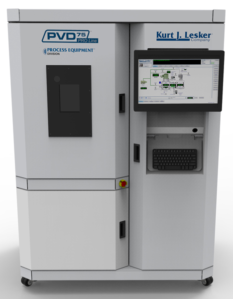
The research utilized several Kurt J Lesker deposition systems[7] and materials to fabricate the thin film layers. A Kurt J. Lesker model PVD75 was used to DC-sputter a Mo film of ~800nm on top of the soda lime glass (SLG) substrate. The CIGS absorber layers were co-evaporated, as per Figure 1, at temperatures shown in Table 1 (below) using a Kurt J Lesker custom made thermal evaporation system. The transparent conductive oxide (TCO) film consisting of a bilayer of 80nm i-ZnO/250nm ITO was sputtered by RF using a PVD75 and the metal contacts were deposited in an electron-beam evaporation PVD75 system (Figure 2).

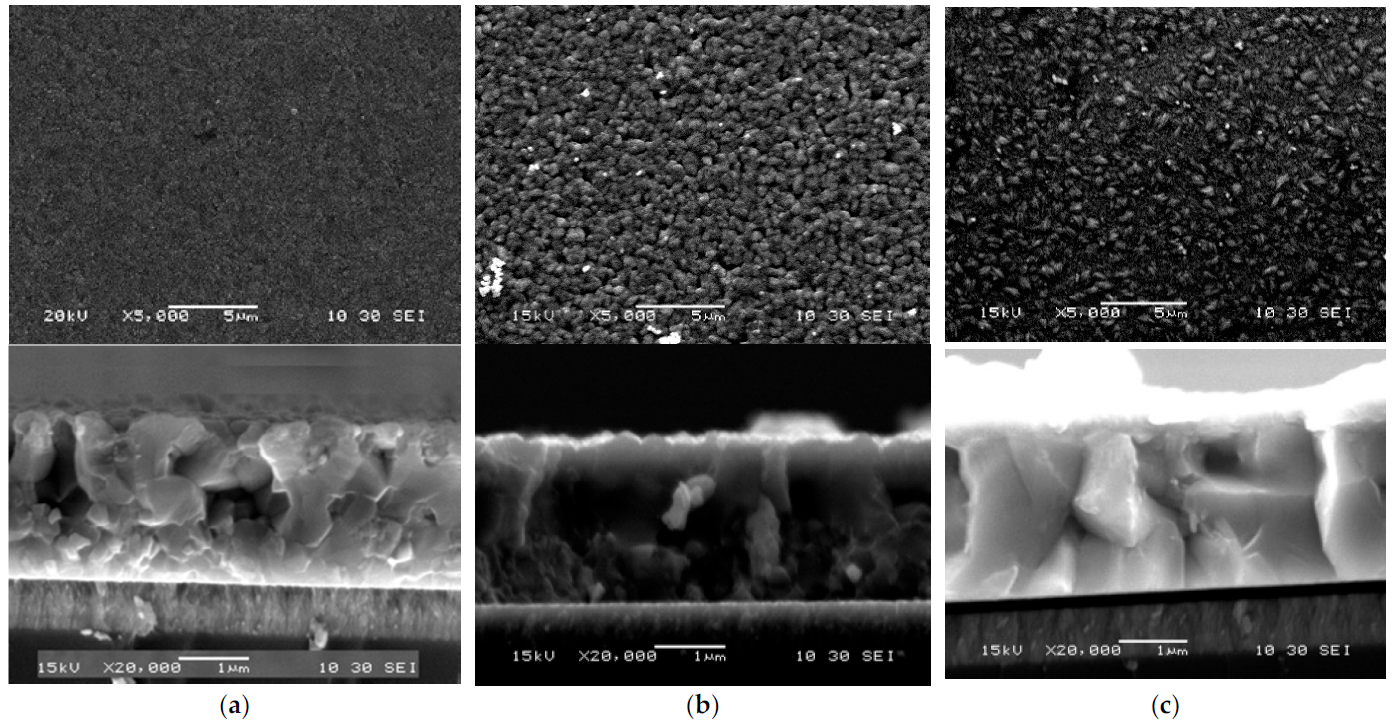
As the first stage temperature was kept constant the CIGS devices were analyzed as a function of the second and third stage temperatures. Using Scanning Electron Microscopy (SEM) to investigate the morphology it was found that those films grown with a higher second stage temperature (HT) exhibited more uniform and compact grain size (Figure 3) than those fabricated at lower temperature (LT).
Looking at the second stage temperature dependence, the group performed X-Ray Diffraction (XRD), X-Ray Fluorescence (XRF) and Secondary Ion Mass Spectrometry (SIMS) analyses on this set of thin films to look at their structure and composition. It was found that deposition temperature effected grain orientation and there was preferential orientation of the HT films, deposited at 400°C, when compared to the LT films, deposited at 350°C, along with a differing distribution of gallium between the two. Both sets of films showed an increase in the level of crystallization. The PV characteristics of the CIGS devices were then measured by current density-voltage (J-V) measurements and external quantum efficiency (EQE) measurements. These revealed a modification of all the parameters listed below after recrystallisation.
- Fill Factor (FF) - a measure of the efficiency of a solar cell
- Open Circuit Voltage (VOC): The highest voltage a solar cell can generate
- Short Circuit Current (ISC): The highest current a solar cell can generate
- Circuit Current Density (JSC): The short circuit current per unit area
It was found that the second stage LT sample had a higher JSC but a lower VOC, even though the band gap was the same as the reference sample. The FF values were the same for both LT sample and reference. The VOC and JSC for the HT samples were similar values to the reference samples but there was an increase in the FF, leading to an overall increase in solar efficiency from 9% to 11%.

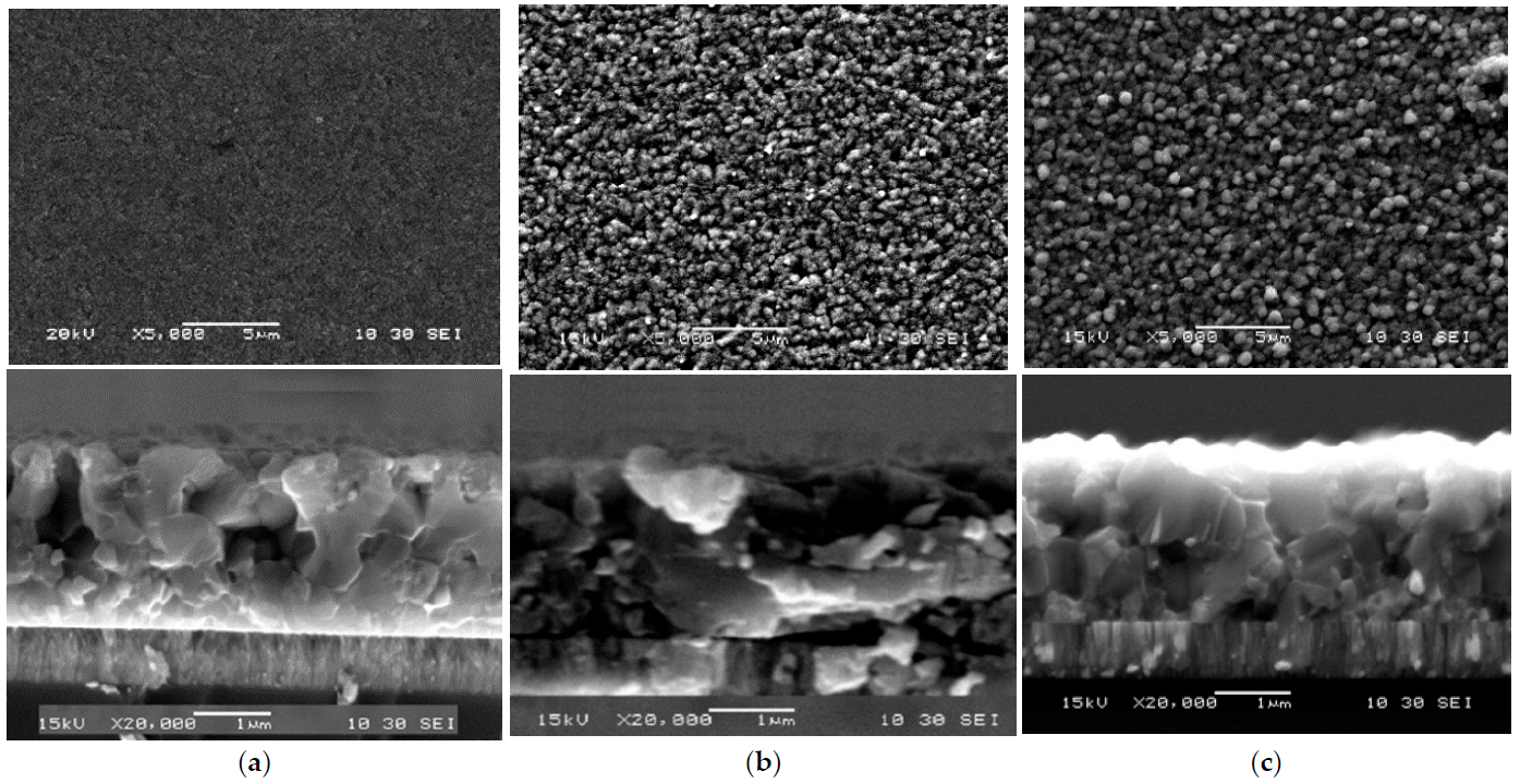
The group then deposited another set of CIGS films, where the second stage temperature was fixed at 400°C, and the third stage was either 425°C (LT) or 450°C (HT) with a fixed first stage temperature of 350oC. An increase in grain size versus the reference sample was found using SEM analysis (see Figure 4). The third-stage HT samples exhibited this effect much more markedly than the LT samples and HT second-stage samples grown at a third stage temperature of 400°C versus 450°C.
The solar cell parameters of the variable temperature third stage CIGS were evaluated using J-V and EQE measurements. It was found that, like the second stage variable temperature samples, that all the parameters were altered after recrystallization, with the FF and EQE values markedly improving. The results are shown in Table 2.

This research clearly shows that by varying the temperature of the second and third stages in this three-stage fabrication process results in selective enhancement of some desirable properties of CIGS PV thin films by majorly affecting the resultant morphology, crystallinity and orientation of the deposited films. Knowing not only how the deposition process parameters fundamentally affects these facets of the films, but also the performance of the devices, is of great importance to the CIGS thin film researcher.
This work has been published in the journal Energies[5].
References:
[1] T. Saga, "Advances in crystalline silicon solar cell technology for industrial mass production", NPG Asia Mater 2, 96-102 (2010). https://doi.org/10.1038/asiamat.2010.82
[2] A. Reinders, P. Verlinden, W. Sark, A. Freundlich, ““Photovoltaic Solar Energy: From Fundamentals to Applications” (2017), Wiley VCH, ISBN: 978-1-118-92746-5
[3] M. A Green, Y. Hishikawa, E. D. Dunlop, D. H. Levi, J. Hohl-Ebinger, A. W. Y. Ho-Baillie, “Solar cell efficiency tables” (version 52). Prog. Photovolt. Res. Appl., 26, 427–436 (2018). https://doi.org/10.1002/pip.3040
[4] Erteza Tawsif Efaz, “A review of primary technologies of thin-film solar cells”, Eng. Res. Express 3, 032001(2021). https://iopscience.iop.org/article/10.1088/2631-8695/ac2353
[5] D. Poudel, B. Belfore, T. Ashrafee, E. Palmiotti, S. Karki, G. Rajan, T. Lepetit, A. Rockett, S. Marsillac, “In Situ Recrystallization of Co-Evaporated Cu(In,Ga)Se2 Thin Films by Copper Chloride Vapor Treatment towards Solar Cell Applications”. Energies, 14, 3938 (2021). https://doi.org/10.3390/en14133938
[6] Weimin Li, Lin Yao, Kaili Li, Xin Li, Bing Yang, Shuda Xu, Sheng Shi, Chenghan Yi, Ming Chen, Ye Feng, Wenjie Li, Ziheng Lu, and Chunlei Yang, “Enabling Low-Temperature Deposition of High-Efficiency CIGS Solar Cells with a Modified Three-Stage Co-Evaporation Process”, ACS Applied Energy Materials, 3 (5), 4201-4207 (2020). http://doi.org/10.1021/acsaem.9b02025
[7] https://www.lesker.com/newweb/vacuum_systems/deposition_systems_pvd_prolinepvd75.cfm
