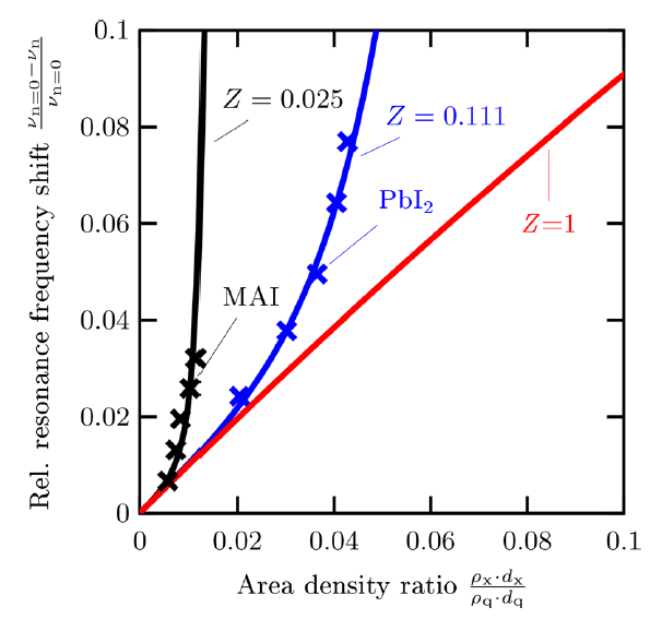
The Kurt J Lesker Company has been shipping Physical Vapor Deposition (PVD) tools into the field of perovskite solar cells for the last decade and continues to support researchers in this exciting application. Our partner, Dr. Sascha J. Wolter, along with the Future Technologies Photovoltaics group, headed by Dr. Sarah Kajari-Schröder, at the Institute for Solar Energy Research (ISFH) in Hamelin, Germany, have presented a method to determine the acoustic impedance ratio (Z) for two perovskite precursors that are commonly co-deposited using PVD. In their paper "Determination and influence evaluation of the acoustic impedance ratio for thermal evaporation"[1] they report Z values for methylammonium iodide (MAI) of 0.025 ±0.002 and 0.11 ±0.01 for lead (II) iodide (PbI2). Furthermore, the impact of using an incorrect Z-ratio on actual experimental thermal evaporations is investigated.

Solar cells work by using materials that absorb photons from sunlight in a broad spectral range and in turn effectively convert this captured light into free charges that produce electricity. Modern commercial solar cells are mainly based on crystalline silicon, which is a cheap and abundant semiconductor[2]. In recent decades thin film technologies such as CIGS, CdTe, amorphous silicon and OPV have all strived to create solar cells that have high efficiencies coupled with good cell stability and low manufacturing costs and come with the advantages of being a thin film by being lightweight and flexible[3]. However, there is a new type of material that has the potential to revolutionize the field of photovoltaics: perovskite-structure based materials. A perovskite structure is any material with the formula ABX3, and it is the recent work centred around metal halide perovskites that has recently garnered a lot of interest in the solar energy world. These easy to fabricate, versatile semiconductors[4] have shown rapid growth in solar cell applications to exhibit electrical power conversion efficiencies (PCEs) from 3.8% to 25.5% over the past few years[5] – which is unprecedented for a solar cell technology and why so many research groups around the world are interested in them.
Metal halide perovskite semiconductors are typically composed of a variety of chemical components comprised of organic and/or inorganic cations, e.g. (for the ABX3 structure), A = methylammonium (MA+), formamidinium (FA+) and Cesium (Cs+); divalent metals e.g., B = lead (Pb2+), tin (Sn2+); and halide anions, e.g. X = iodide (I-), bromide (Br-) and chloride (Cl-)[6]. With a wide range of band-gaps, tunable by the chemical composition, they are well suited for all-perovskite tandem solar cell configurations[7] or being combined with existing silicon technologies[8].
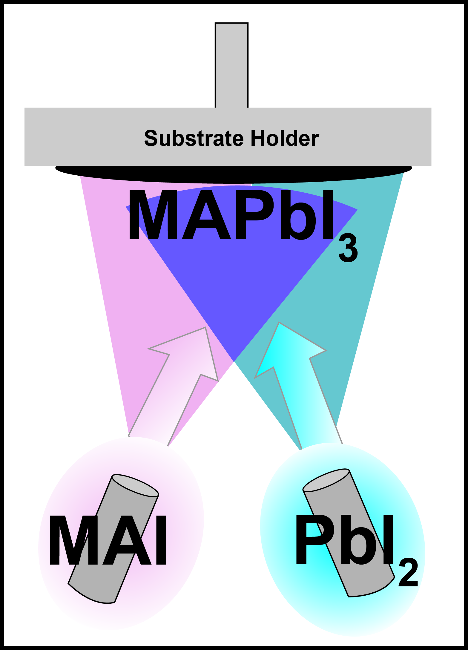
The thermal co-evaporation of perovskite precursors can result in a conformal thin film with homogeneous layer thickness if key control parameters are understood and met. A key parameter is the deposition rate, which is commonly measured by using a quartz crystal microbalance. This method is efficient for the accurate measurement of the deposition rate of common materials. However, for organic perovskite precursors like MAI, quartz crystal sensor readings can prove to be problematic mainly due to the omnidirectional behavior of the evaporation flux. Additionally, the impurities in the organic precursor can highly influence the deposition on the quartz crystal[9]. Several groups have looked at alternative ways of measuring the deposition rate of perovskite precursors with varying degrees of success[10,11,12], but the measurement of film thickness and rate by quartz crystal sensor is an industry-standard approach for vacuum coating, so the ability to go this route is important, especially for scaling up to larger production scale size substrates.
For the successful thermal co-evaporation of perovskite precursors, a constant deposition rate is necessary. For the quartz crystal sensor head to read an accurate film value and thus deposition rate to be calculated, the density, ρ, and the acoustic impedance ratio of the material, Z, must be known for the evaporant. Unfortunately, often the values of ρ and Z are rarely known for organic perovskite materials[13], so knowing this is of vital importance for successful co-evaporation, otherwise there is a mismatch between the measured and actual deposited film thickness.
The density of a material can be determined by an immersion experiment, so the ISFH researchers first looked at measuring the density of the MAI by adding a known mass of MAI to a certain volume of diethylether in a glass tube and measuring the change in the fill level. Using this method, they reported the density ρMAI to be an average of 2.95 ±0.28 gcm-3.
To determine the acoustic impedance ratio the ISFH team then made the assumption of a composite resonator in their approach. Using a glovebox-integrated Kurt J Lesker Mini SPECTROS™ tool they deposited five sequential layers of MAI or PbI2 onto a single quartz crystal, located in the process chamber, to determine the acoustic impedance ratio. After each layer deposition the resonance frequency of the quartz crystal was measured along with the thickness of material deposited. This was achieved by using scanning electron microscopy (SEM) of a silicon substrate loaded in a substrate holder in the same process chamber. The data obtained was then fitted to the composite resonator model and produced best fit results of an acoustic impedance ratio of 0.025 ± 0.002 for MAI and of 0.110 ± 0.01 for PbI

*Photo: ISFH, taken by Salzmann-Fotografie*
Utilizing the calculated impedance ratios, the ISFH team then deposited a layer of MAPbI3 onto a 2.5cm2 silicon substrate using the Mini SPECTROS, co-evaporating MAI and PbI3 from Low Temperature Evaporation (LTE) sources, aiming for a I:Pb ratio of 3:1 in the resultant film. Measured using SEM and X-ray diffraction the film was observed to be columnar and crystalline. Using energy dispersive X-ray spectroscopy, the atomic ratio of I:Pb was measured to be 3.2 ± 0.2 which proved the effectivity of using the new acoustic impedance ratios by achieving an excellent control of the deposited film's chemical composition.
Normally the general assumption is that the acoustic impedance of organic perovskite precursors is 1 or similar[14]. The ISFH team then investigated the issues with this assumption by modelling the deposition layer thickness with the calculated Z values of MAI and PbI2 relative to when this value is 1, both in terms of the layer thickness predictions but also the actual stoichiometry of the deposited films. The results are shown in Figure 4.


The research clearly showed that the use of Z = 1 for the deposition of these materials is not recommended to enable accurate and controlled thermal co-evaporation process control conditions and the impact of the wrong Z value has a large impact on the experimental results, e.g. a changing composition of the perovskite over the layer thickness.
This work has been published in Applied Physics Letters. The group from ISFH will use these important findings to look at large area deposition of perovskite materials in tandem solar cell applications in the future.
References:
[1] S. Wolter, V. Steckenreiter, M. C. Tatarzyn, T. Wietler, R. Niepelt, S. Kajari-Schröder, "Determination and influence evaluation of the acoustic impedance ratio for thermal coevaporation", Appl. Phys. Lett. 113, 013301 (2018). https://doi.org/10.1063/1.5037403
[2] T. Saga, "Advances in crystalline silicon solar cell technology for industrial mass production", NPG Asia Mater 2, 96–102 (2010). https://doi.org/10.1038/asiamat.2010.82
[3] S. Hegedus, "Thin film solar modules: the low cost, high throughput and versatile alternative to Si wafers", Progress in Photovoltaics, (2006). https://doi.org/10.1002/pip.704
[4] S. Stranks, H. J. Snaith, "Metal-halide perovskites for photovoltaic and light-emitting devices", Nat. Nanotechnol, 10, 391, (2015). https://doi.org/10.1038/nnano.2015.90
[5] https://www.nrel.gov/pv/assets/pdfs/best-research-cell-efficiencies.20200925.pdf, accessed 7th December 2020.
[6] S. F. Hoefler, G. Trimmel, T. Rath, "Progress on lead-free metal halide perovskites for photovoltaic applications: a review", Monatsh Chem 148, 795–826 (2017). https://doi.org/10.1007/s00706-017-1933-9
[7] D.P. McMeekin, G. Sadoughi, W. Rehman, G. E. Eperon, M. Saliba, M. T. Hörantner, A. Haghighirad, N. Sakai, L. Korte, B. Rech, M. B. Johnston, L. M. Herz, H. J. Snaith, "A mixed-cation lead mixed-halide perovskite absorber for tandem solar cells". Science, 351, 151-155, (2016). https://doi.org/10.1126/science.aad5845
[8] M. Anaya, G. Lozano, M. E. Calvo, H. Míguez, "ABX3 Perovskites for Tandem Solar Cells", Joule, 1, 431, (2017). https://doi.org/10.1016/j.joule.2017.09.017
[9] J. Borchert, I. Levchuk, L. C. Snoek, M. U. Rothmann, R. Haver, H. J. Snaith, C. J. Brabec, L. M. Herz, M. B. Johnston, "Impurity Tracking Enables Enhanced Control and Reproducibility of Hybrid Perovskite Vapor Deposition", ACS Appl. Mater. Interfaces 11, 28851–28857 (2019). https://doi.org/10.1021/acsami.9b07619
[10] L. K. Ono, S. Wang, Y. Kato, S. R. Raga, Y. Qi, "Fabrication of semi-transparent perovskite films with centimeter-scale superior uniformity by the hybrid deposition method", Energy Environ. Sci, 12, 3989–3993 (2014). https://doi.org/10.1039/C4EE02539C
[11] S. Wang, L. K. Ono, M. R. Leyden, Y. Kato, S. R. Raga, M. V. Lee, Y. Qi, "Smooth perovskite thin films and efficient perovskite solar cells prepared by the hybrid deposition method", J. Mater. Chem. A, 3, 14631–14641 (2015). https://doi.org/10.1039/C5TA03593G
[12] C. Momblona, L. Gil-Escrig, E. Bandiello, E. M. Hutter, M. Sessolo, K. Lederer, J. Blochwitz Nimoth, H. J. Bolink, "Efficient vacuum deposited p-i-n and n-i-p perovskite solar cells employing doped charge transport layers," Energy Environ. Sci. 9, 3456–3463 (2016). https://doi.org/10.1039/C6EE02100J
[13] L. K. Ono, M. R. Leyden, S. Wang, Y. Qi, "Organometal halide perovskite thin films and solar cells by vapor deposition", J. Mater. Chem. A, 4, 6693–6713 (2016). https://doi.org/10.1039/C5TA08963H
[14] M. Liu, M. B. Johnston, H. J. Snaith, "Efficient planar heterojunction perovskite solar cells by vapour deposition", Nature 501, 395–398 (2013). https://doi.org/10.1038/nature12509


