Silicon Si (P-type) Evaporation Process Notes
Silicon is one of the most extensively used elements in the world. It is dark gray and semi-metallic with a bluish tinge. It has a melting point of 1,410°C, a density of 2.32 g/cc, and a vapor pressure of 10-4 Torr at 1,337°C. It is a brittle metalloid which can chip easily. Silicon is a semiconductor which is heavily utilized in the electronics and computer industries. It is often doped with arsenic, phosphorus, or boron depending on the application. It is evaporated under vacuum for circuit device, data storage device, and battery fabrication.
Silicon Si (P-type) Specifications
| Material Type | Silicon (P-type) |
| Symbol | Si (P-type) |
| Atomic Weight | 28.0855 |
| Atomic Number | 14 |
| Color/Appearance | Dark Gray with a Bluish Tinge, Semi-Metallic |
| Thermal Conductivity | 150 W/m.K |
| Melting Point (°C) | 1,410 |
| Bulk Resistivity | 0.005-0.020 OHM-CM |
| Coefficient of Thermal Expansion | 2.6 x 10⁻⁶/K |
| Theoretical Density (g/cc) | 2.32 |
| Sputter | DC, RF |
| Max Power Density (Watts/Square Inch) | 40* |
| Type of Bond | Indium, Elastomer |
| Dopant | Boron |
| Z Ratio | 0.712 |
| E-Beam | Fair |
| E-Beam Crucible Liner Material | FABMATE®‡, Tantalum |
| Temp. (°C) for Given Vap. Press. (Torr) |
10-8: 992 10-6: 1,147 10-4: 1,337 |
* This is a recommendation based on our experience running these materials in KJLC guns. The ratings are based on unbonded targets and are material specific. Bonded targets should be run at lower powers to prevent bonding failures. Bonded targets should be run at 20 Watts/Square Inch or lower, depending on the material.
Z-Factors
Empirical Determination of Z-Factor
Unfortunately, Z Factor and Shear Modulus are not readily available for many materials. In this case, the Z-Factor can also be determined empirically using the following method:
- Deposit material until Crystal Life is near 50%, or near the end of life, whichever is sooner.
- Place a new substrate adjacent to the used quartz sensor.
- Set QCM Density to the calibrated value; Tooling to 100%
- Zero thickness
- Deposit approximately 1000 to 5000 A of material on the substrate.
- Use a profilometer or interferometer to measure the actual substrate film thickness.
- Adjust the Z Factor of the instrument until the correct thickness reading is shown.
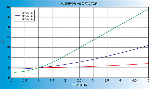
Another alternative is to change crystals frequently and ignore the error. The graph below shows the % Error in Rate/Thickness from using the wrong Z Factor. For a crystal with 90% life, the error is negligible for even large errors in the programmed versus actual Z Factor.


