J.R. Gaines, Jr. Technical Director of Education for the Kurt J. Lesker Company
Introduction
High impulse power magnetron sputtering, either HIPIMS or HiPMS, was first reported in 1999 by Dr. Vladimir Kouznetsov, et al. from Linköping University’s Department of Physics. HIPIMS is distinct from classical direct current magnetron sputtering, or dcMS, because it utilizes a rapid series of pulses at very high voltage, on the order of 2000V, and high current density approaching 10A/cm2. In addition, HIPIMS also exhibits some degree of self-sputtering, where sputter target adatoms are ionized with some recycling of process gas and ionized target material to the surface of the target. More recently, HIPIMS power supplies have been re-engineered to provide both negative AND positive pulses to the target [ref. 1]. This advance has enabled new flexibility on the application of HIPIMS to a variety of thin film growth challenges.
Comparing Direct Current Magnetron Sputtering (dcMS), Pulsed dcMS and High Impulse Power Magnetron Sputtering (HIPIMS)
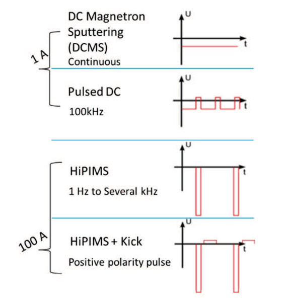
The pulses in HIPIMS can be two orders of magnitude larger than in pulsed DC magnetron sputtering (Figure 1). Recent innovations in the HIPIMS cycle include a positive pulse at the face of the target. [Ref. 1] This approach serves to eject or exclude trapped sputter target ions that may been recycled to the surface of the target, engaged in self sputtering so that, once rejected they can then contribute to the flux of adatoms heading to the surface of the substrate. In addition, the expanding plasma can ionize some of the sputtered atoms which are in route to the substrate. Work by Ruzic, et al… suggests that the number of the highly energetic ions incident to the substrate is increased by more than 18%. [Ref. 1].
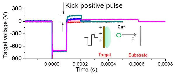
The pulsed kick is variable in terms of voltage and pulse length which enables new parameters to further tune thin film properties (see Figure 2). This introduces a new level of material-specific process conditions which enable the user to further customize the morphology of their films.
System diagram
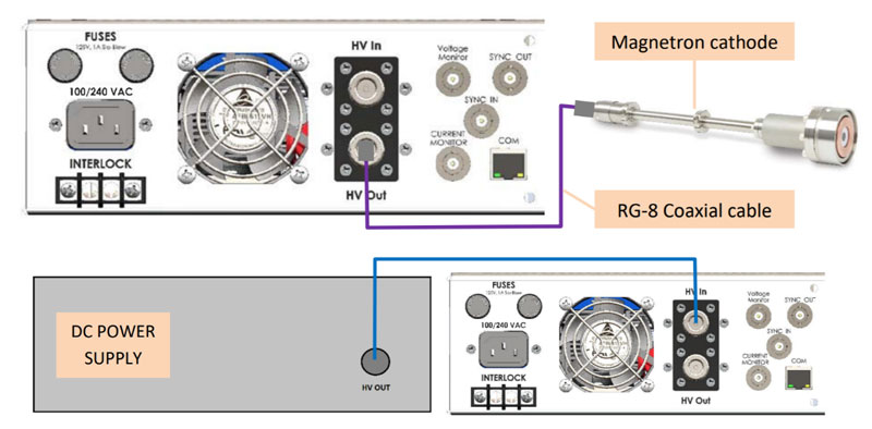
The following graphic (see Figure 3) details one possible system set-up for the conversion of a traditional direct current magnetron sputtering power supply to a HIPIMs source through the addition of an "impulse" power supply, in this case a Starfire Industries model 2-2. For the deposition of copper films [Ref. 1] a typical set of discharge parameters include a voltage of 710 V, a pulse duration of 100 µS and a frequency of 600 Hz. The cathode is a TORUS® UHV compatible Mag Keeper circular magnetron sputter source.
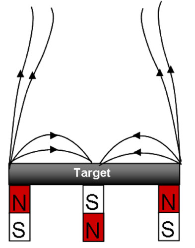
The HIPIMS enhanced thin film deposition approach benefits from the use of an unbalanced magnetron configuration. In the unbalanced design the cathode utilizes a range of high power magnets with the group which makes up the edge fields are significantly more energetic than the center magnets. This helps distort some magnetic field lines so that they are more normal to the substrate surface. This enables a pathway for the secondary electrons created as an artifact of ionized collisions of the process gas (and self-sputtered target ions) to travel to the substrate and continue to help promote ionization of both process and target adatoms (see Figure 4).
Substrate preparation
Substrate preparation is critical in order to minimize the possibility of contaminant inclusions and stacking layer defects in thin films. While there are some heroic efforts that can be utilized to prepare a substrate at atmosphere, in a clean room, the most effective routes include in-situ, in high vacuum, under energetic and pristine conditions where unwanted species on surfaces can be ablated off the surface of substrates and into the pumping system. HIPIMS enables the use of high energy pulses to both ablate substrate surfaces of tramp species such as water and hydrogen, as well as develop an inter-mix layer of metal ions and substrate may enhance film adhesion and reduce stress. The formation of a mixed material interface layer helps to functionalize the substrate and mitigate what may be competing attractions between the film and substrate.
Humans are notoriously incompetent when it comes to substrate preparation. In the hundreds of lectures on vacuum science I have delivered when I pronounce that nothing going into a vacuum chamber, including substrates, can ever have been touch be human hands, I see a room full of students look like deer in the headlights. HIPIMS enables the aggressive cleaning, using an argon plasma below 32 eV, or whatever the sputtering threshold is, followed by a pulse of energetic target ions which, above 32 eV and more likely close to 100 eV, may penetrate the substrate surface and create a mixed interface layer of film/substrate which reduces the possibility of an abrupt break between the as-deposited form and the substrate.
Deposition rate
Despite the enhanced film properties achievable with conventional HIPIMS, the technology has been held back from wide spread adoption by the decreased deposition rate achieved for most metals. However, in work done at the Center for Plasma-Material Interactions (CPMI) at the University of Illinois in Urbana Champaign, the addition of the positive kick in the HiPMS process cycle was shown to increase rates (see Figure 5) by more than 15% [Ref.1]. The kick pulse, with its positive charge, forces ions that have recycled to the target surface to be forced toward the substrate.
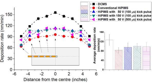
Altering the magnet pack with one specifically designed for HIPIMS can increase this rate even more [Ref.15] and can even exceed the DC sputtering rate for some cases.
Tunable ion energy distribution & argon to metal ion ratio
There are several models of thin film structures published which intend to integrate various factors, such as base pressure, substrate bias, the ratio of substrate temperature to the melting temperature of the material, and energy of the arriving adatoms on morphology. There may be a need to update these models to include the additional morphologies achievable with high power pulsing approaches. The ability to tune the HIPIMS process for specific materials and morphologies adds another tool in the chest of sputtering metal thin films. Researchers have demonstrated that tuning the voltage and duration parameters of the positive kick can substantially effect thin film characteristics like density, stress and grain size.
Ruzic, et al, [Ref. 1] report an 18% increase in the number of ions at the surface of the substrate when using the positive kick for deposition of copper on silicon. Ion velocities at 6 cm distance from the source are on the order of 2,500 meters/second. [Ref. 5].
By studying the temporal evolution of the pulsed plasma, which initiates with a predominantly Ar rich composition but then, at the end of the pulse, transitions to a metal ion plasma, selective biasing of the substrate can be used to select metal or Ar ions with which to bombard the substrate.
Self-sputtering
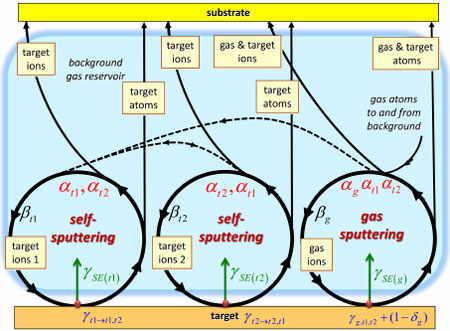
In his brief review titled “The Discharge Physics of High Power Impulse Magnetron Sputtering,” [Ref. 6] Dr. André Anders describes a special case of ‘gasless’ self-sputtering. In HIPIMS-induced self-sputtering a substantial portion of the atoms ejected from the sputter target get ionized. The fraction is so high the process gas atmosphere in the vicinity of the target gets rarefied to the exclusion of the process gas. If the sputter plasma is dominated by a high enough fraction of sputter target ions targets are self-sputtering can enter a self-sustaining mode at which time the traditional working gas of the system can be eliminated (see Figure 6). Further, with the addition of the positive kick feature, sputter target ions heading back toward the target can be ejected from the area at the target surface and repelled toward the substrate.
3D conformal deposition
Sputtering is a relatively high pressure process for thin film deposition. Thermal and e-Beam evaporation, Molecular Beam Epitaxy as well as Pulsed Laser Deposition are done at pressures, on the order of 10-7 Torr or less, which are sufficiently low that the mean free path, or the average distance that one molecule has to travel before it collides with another, of the tramp gases in the deposition chamber is substantially larger than the source-to-substrate distance. While the arriving adatoms from these processes only have thermal energies and are likely to need an assist in order to make dense films, they are less likely to contain gas inclusions/defects and more likely to arrive with an incident angle normal to the substrate, or at some controlled angle for processes such as Glancing Angle Deposition or GLAD [Ref. 7]. The high pressure process gases in sputtering and the string of collisions likely for a sputter target molecule on its way to a substrate, cause the incident angle of the arriving material to be quite random. As these adatoms have, generally, a neutral charge, they arrive at the substrate with no preferential angles. This effects characteristics such as sticking coefficients and layer formation.
Traditional HIPIMS generates significant numbers of sputter target ions which can be substantially influenced with substrate bias. For the population of sputter target ions arriving at the substrate there are a host of beneficial characteristics that can be tailored. At some critical voltage, the substrate bias can be tuned such that incident angle of the arriving ions are more likely to be normal to the substrate. For example, thin film conformity on high aspect ratio substrates can be enhanced by a positive kick which substantially increases the number of sputter target ions at the substrate and in conjunction with a bias can have those ions arrive at an incident angle more normal to the substrate. Depositing conformal coatings in deep trenches has always been a challenge. Approaches like atomic layer deposition (ALD) have been useful for material/precursor reactions that can be brought to completion with heat but they are less effective with deep trenches. In the case of most metals, a process called Plasma Enhanced ALD is required to drive the chemical reactions between precursors but the plasma dissipates with the depth of the via.
The addition of a positive kick to the HIPIMS cycle enables the rejection of the remaining sputter target ions at the surface of the source forcing them toward the substrate. In work done by Ruzic et al… [Ref. 13] they estimate that the flux of target material at the substrate is increased by more than 18%. By sending a large fraction of ionized sputter target material to the substrate the positive kick pulse boosts the deposition rate of HIPIMS and also contributes more energy to the film that can contribute to adatom mobility.
In the case where a substrate can be biased the incident angle of the arriving adatoms may be influenced so that their arrival is predominantly normal to the substrate and/or electrically attracted to any available site on the substrate. While there may be alternative methods to effectively coating deep trenches, HIPIMS near the self-sputtering limit, adds something more than line-of-site collision paths to this high pressure deposition technique.
Extremely smooth thin films
Thin film features such as smoothness are highly dependent on the energies of the arriving adatoms. The more energetic the adatom the more likely it has sufficient mobility at the substrate film interface to move around and fill any available open site in the current monolayer. Of course there is a sweet spot between weakly energetic adatoms which will make course films and over energetic species that will active etch the film and substrate. With HIPIMS, energies can meet or exceed 100 eV.
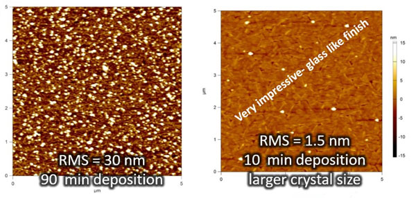
Work done by J.P. Maria while at North Carolina State University demonstrated extremely smooth and also thick films by use of a positive kick in the traditional HIPIMS cycle (see Figure 7). In his work to make high quality plasmonic thin films of doped cadmium oxide he was able to substantially increase film density and smoothness due to the high flux of very energetic sputter target ions at the substrate.
Deposition of dense films on insulating/semiconductive substrates
The ability to kick, or reject sputter target ions from the surface of the source assures that a large number of charged adatoms are forced to the substrate. This enables to use of insulating or semiconductive substrates that cannot be effectively biased. Because the sputter target ions are being kicked they can get to the substrate without the influence of a charge at the film/substrate interface. With the additional 18% of ions getting to the substrate films are likely to be more dense, and with the extra energy available, on the order of 100 eV, arriving adatoms have plenty of mobility and are more likely to form monolayers. [Ref. 9]
Improved sp3 content in Diamond-like carbon thin films
The wholly grail of diamond-like carbon (DLC) coatings is to maximize the content of sp3 in arbitrarily thick films. The four valence electrons of carbon allow it to appear in three hybridization states: sp3, which is the predominate species in diamond; sp2, which is the stuff of graphite; and sp, which is similar to alkaline. The sp3 orbital is the version most dominant in diamonds – as such, the most sought after for hardness, thermal conductivity and optical films. HIPIMS has been successfully employed to make DLC films and the extreme energetics created in the process seem to have a positive impact of sp3 formation [Ref. 10]. One reason that HIPIMs has been so successful is the enormous energies achieved in individual pulses AND the ability to specifically tune the pulse peaks to optimize material-specific characteristics – like phase formation (see Figure 8).
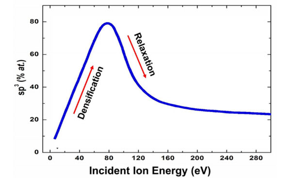
In work done by Tell at Uppsala Universitet, [Ref.11] the optimal subplantation energy for the sp3 carbon phase was found to be 80 eV. The minimum was about 32 eV, but by tuning the energy of the pulse the sp3 content of the thin films was increased to 80%. At energies in excess of 80 eV the surface of the films relaxes and the sp3 content decreases.
In addition to an opportunity to improve the fraction of sp3 in DLC, the inclusion of the positive kick in the HIPIMs cycle enables the production of films which are substantially smoother than dcMS of traditional HIPIMS alone (see Figure 9) [Ref. 12]
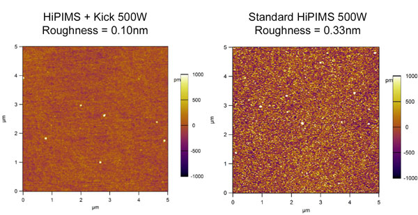
Additionally, the authors report an 11% increase in film density between the HIPIMS plus kick and the traditional HIPIMS process. Further, films made by the HIPIMS + kick method were further optimized to increase density in DLC films.

Summary
The addition of a tunable positive kick feature to the traditional HIPIMS cycle has enabled several advances to what had already been an important new tool in the deposition of high quality thin films. Embraced for a wide variety of applications, several research groups have reported improvements in their films including:
- Substrate cleaning and functionalization
- Deposition rate
- Selective argon or sputter target ion bombardment with controlled energy
- Self-sputtering
- Conformal coatings on 3 dimensional substrates
- Film smoothness
- Dense films on insulating or semiconductive substrates which cannot be bias
- Increased sp3 content in diamond-like carbon films
- Controlling the stress in a film [Ref. 14]
Likely, as HIPIMS enhanced by a positive kick achieves widespread adoption there will be other benefits revealed. For example, it appears that the optimal design of the pulse, in voltage and duration, may be material specific. So as this approach is expanded to the entire suit of electrically conductive materials that are utilized as thin films, additional new morphologies of popular materials may be discovered. Certainly improvements in fundamental properties such as density, adhesion, and smoothness are likely to be demonstrated in most conductive thin film materials.
References:
- Cu films prepared by bipolar pulsed high power impulse magnetron sputtering, B Wu, I. Haehnlein, I Shchelkanov, J. McLain, D. Patel, J. Uhlig, B. Jurczyk, Y. Leng, D. Ruzic, Vacuum 150 (2018) 216-221
- Low Friction and Wear Resistant Carbon Nitride Thin Films for Rolling Components, Thesis by Konstantinos D. Bakoglidis, Linkoping University Institute of Technology, 2015.
- Structural Investigations of HIPIMS-Deposited Diamond Like Carbon Thin Films using Raman Spectroscopy, Andreas Eriksen Tell, Uppsala Universitet, April 2017
- Stress and Texture in HIPIMS TiN Thin Films, Machunze, et al… Delft University of Technology, Thin Solid Films, 2009.
- Ionized sputter deposition using an extremely high plasma density pulsed magnetron discharge, K. Macak, V. Kouznetsov, J. Schneider, U. Helmersson and I. Petrov, Journal of Vacuum Science & Technology A 18, 1533 (2000)
- Discharge Physics of High Power Impulse Magnetron Sputtering, André Anders, Surface and Coatings Technology, October 13, 2010.
- Sculptured thin films and glancing angle deposition: Growth mechanics and applications, K. Robbie and M.J. Brett, Journal of Vacuum Science & Technology A 15, 1460 (1997)
- Photonically Tunable MIR Epsilon-Near Zero Modes in CdO Thin Films, E. Radue, E. Runnerstrom, K. Kelley, J.P. Maria & P. Hopkins, conference paper, Laser Science 2018, Washington, DC, 16 – 20 September 2018, poster session II (jTu3A)
- Private communication, Brian Jurczyk, Starfire Industries, August 7, 2018
- HIPIMS-based Novel Deposition Processes for Thin Films, Asim Aijaz, Linköping University Institute of Technology, Plasma & Coatings Physics Division, Licentiate Thesis No. 1537
- Structural Investigations of HIPIMS-deposited Diamond-Like Carbon Thin Films using Raman Spectroscopy, Andreas Eriksen Tell, Uppsala Universitet, April 2017.
- High sp3 DLC with iPVD through Modified High Impulse Magnetron Sputtering, I. Haehnlein, B. Wu, E. Barlaz, J. McLain, B. Jurczyk, D. Ruzic, Center for Plasma-Material Interaction, presented at HIPIMS 2018, Sheffield, UK, June 27th, 2018
Additional references:
- Baohua Wu, Yan Yu, Jian Wu, Ivan Shchelkanov, David N. Ruzic, Nan Huang, Y.X. Leng, “Tailoring of titanium thin film properties in high power pulsed magnetron sputtering”, Vacuum 150, 144-154 (2018).
- J. McLain, P. Raman, D. Patel, R. Spreadbury, J. Uhlig, I. Shchelkanov, D. N. Ruzic,, “Linear Magnetron HIPIMS High Deposition Rate Magnet Pack”, Vacuum 155, 559-565 (2018).
- P. Raman, I.A. Shchelkanov, J. McLain, D.N. Ruzic, “High power pulsed magnetron sputtering: A method to increase deposition rate”, J. Vac. Sci. Technol. A 33(3), May/Jun (2015).
- P. Raman, I. Shchelkanov, J. McLain, M. Cheng, D. N. Ruzic, I. Haehnlein, B. Jurczyk, R.Stubbers, S. Armstrong, “High deposition rate symmetric magnet pack for high power pulsed magnetron sputtering”, Surf. Coat. Technol. 293, 10 (2015).
